

Semiconductor photodetector
a photodetector and semiconductor technology, applied in the field of semiconductor photodetectors, can solve the problems of extremely low s/n ratio given by the ratio of signal (s) and noise (n), high dark noise of the semiconductor photodetector, and high noise of multiplication
- Summary
- Abstract
- Description
- Claims
- Application Information
AI Technical Summary
Benefits of technology
Problems solved by technology
Method used
Image

Examples
first exemplary embodiment
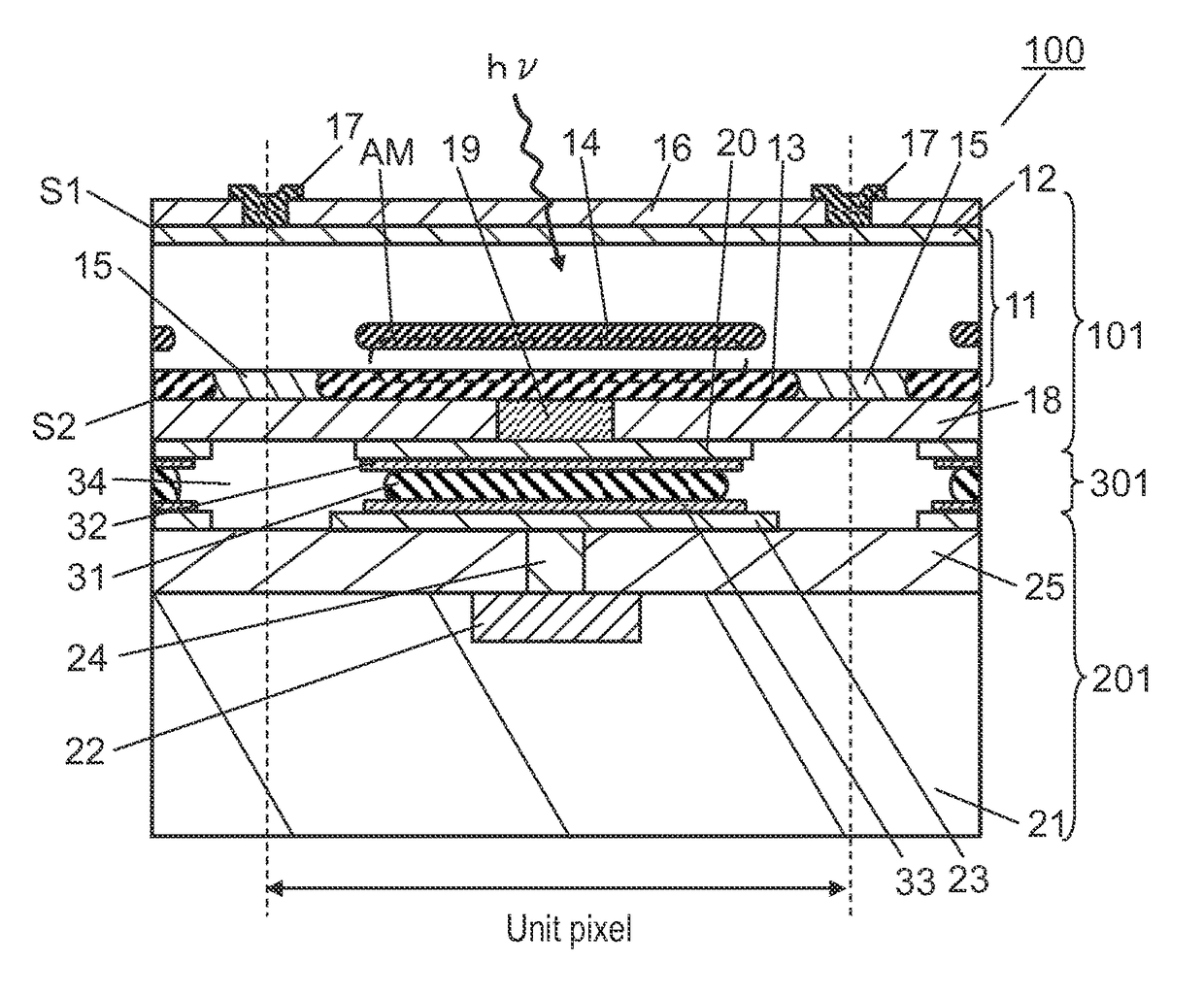
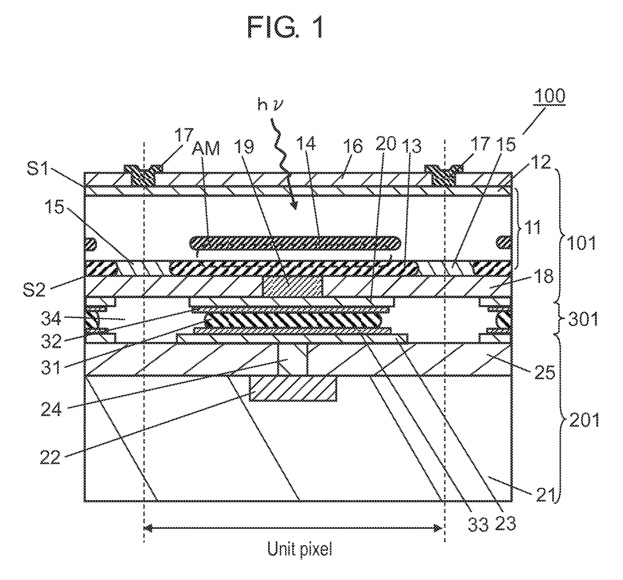
[0043]First, with reference to FIG. 1 and FIG. 2, there will be described a structure of a unit pixel of a semiconductor photodetector according to a first exemplary embodiment of the present disclosure. FIG. 2 is a partial transparent drawing for clearly illustrating an arrangement, in a planar view, in the semiconductor photodetector according to the present exemplary embodiment. Note that the term “planar view” in the present detailed description represents the view from the normal line direction of a light receiving surface of photoelectric conversion part 101.
[0044]Semiconductor photodetector 100 according to the present exemplary embodiment has a plurality of unit pixels arranged, in a matrix, on semiconductor substrate 21. Each of the plurality of unit pixels has photoelectric conversion part 101 and detection circuit 201, and photoelectric conversion part 101 and detection circuit 201 are electrically connected through bonding part 301.
[0045]First, photoelectric conversion p...
second exemplary embodiment
[0130]With reference to FIG. 13 and FIG. 14, there will be described a structure of a unit pixel of semiconductor photodetector 500 according to a second exemplary embodiment of the present disclosure.
[0131]Semiconductor photodetector 500 according to the present exemplary embodiment is provided, in a matrix, with a plurality of unit pixels on semiconductor substrate 516. Each of the plurality of unit pixels has photoelectric conversion part 502 and detection circuit 504; and photoelectric conversion part 502 and detection circuit 504 are electrically connected through pixel electrode 506 and contact plug 514.
[0132]Photoelectric conversion part 502 is constituted of semiconductor part 508 made of a photoconductive material. Electrode 510 is formed on a surface of semiconductor part 508, where incident light enters.
[0133]Examples of the photoconductive material include a semiconductor containing Se, a compound semiconductor CuInxGa1-xSySe1-y (where 0≦x≦1 and 0≦y≦1), and group III-V c...
PUM
 Abstract
Description
Claims
Application Information