

Photodiode type structure, component and method for manufacturing such a structure
a photodiode and semiconductor technology, applied in the field of photodiodes, can solve the problems of degrading the signal to noise ratio of such a structure, unable to achieve auger phenomena, and subjected to important nois
- Summary
- Abstract
- Description
- Claims
- Application Information
AI Technical Summary
Benefits of technology
Problems solved by technology
Method used
Image

Examples
first embodiment
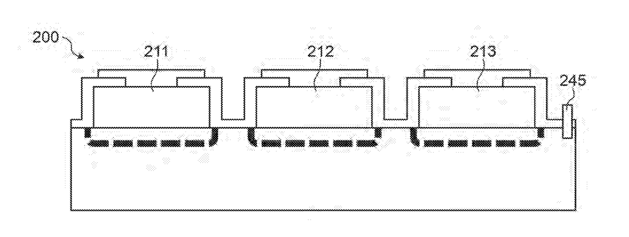
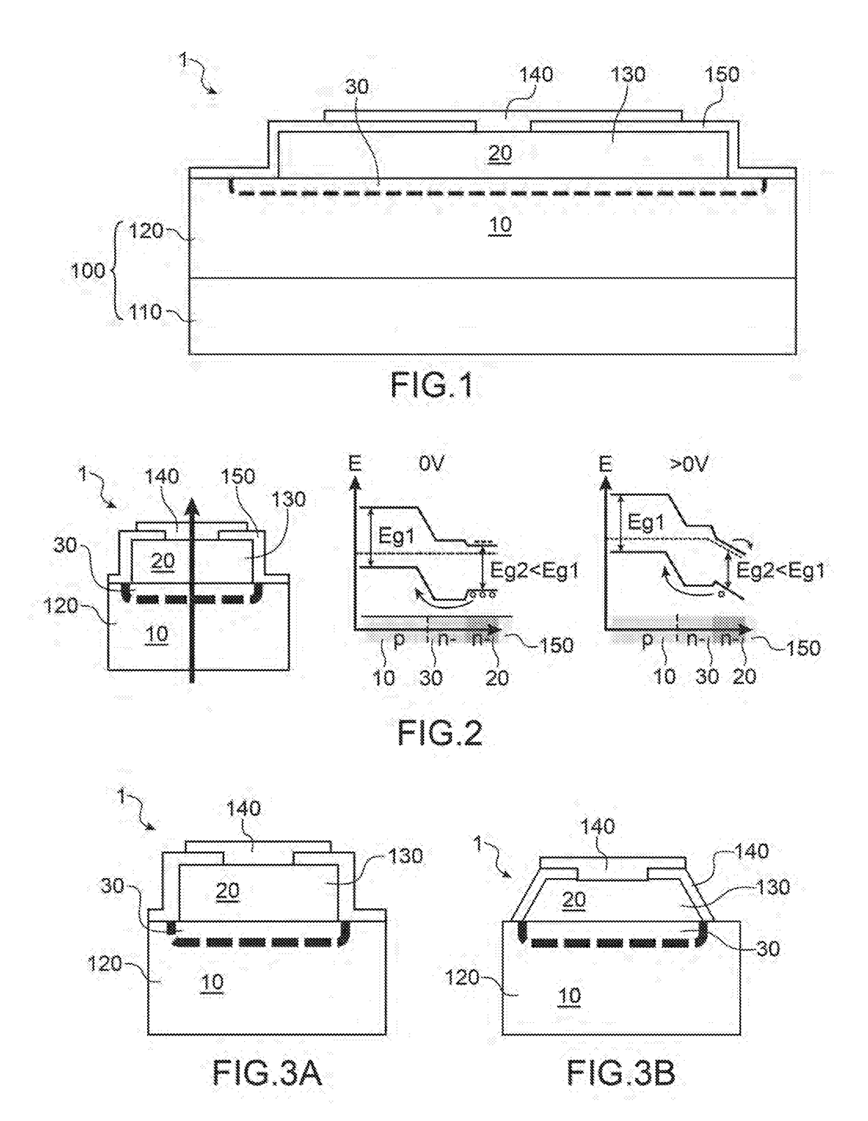
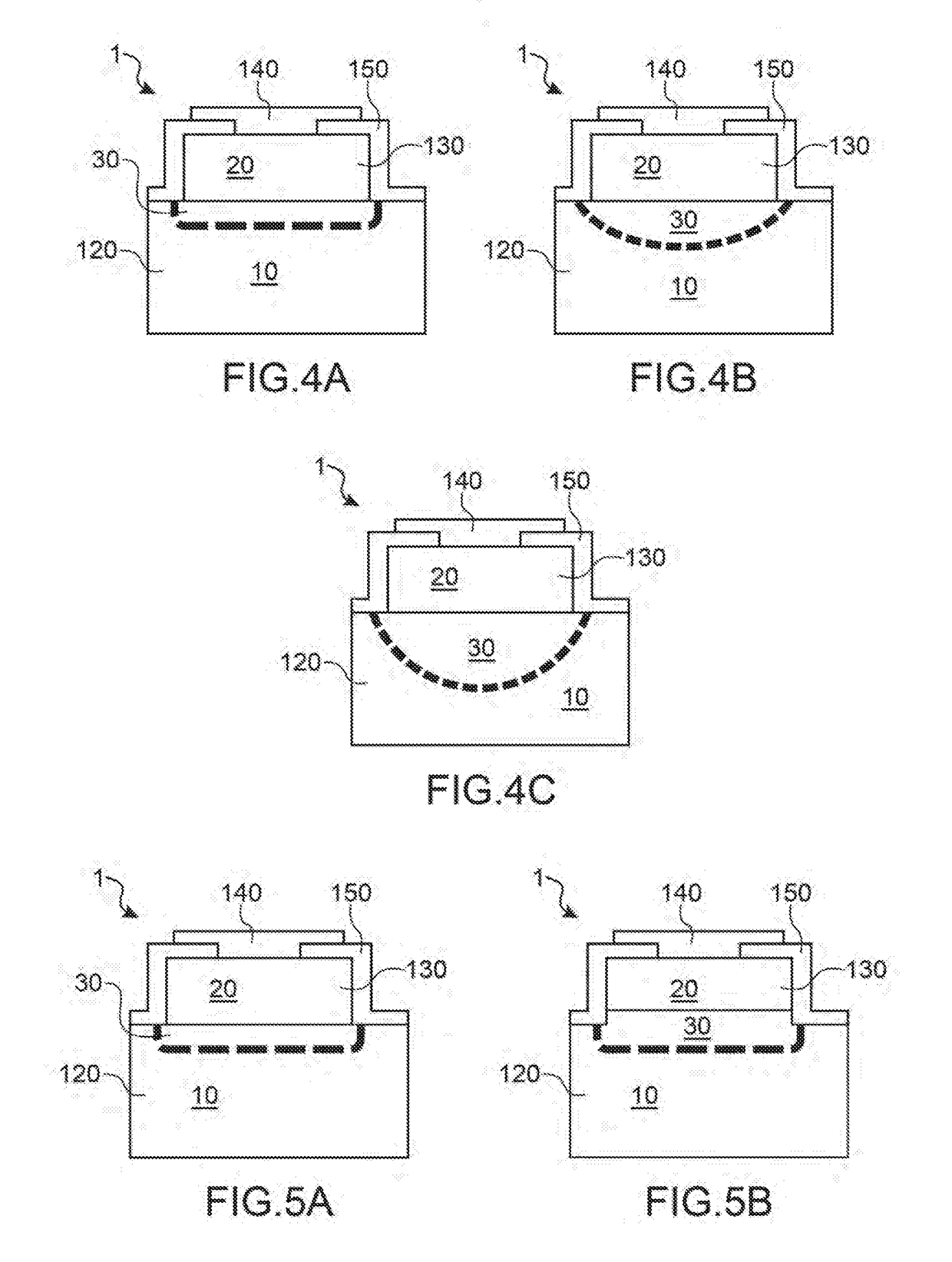
[0148]FIGS. 5A and 5B illustrate two possibilities of the invention concerning the positioning of the third zone 30. In fact, as described above in this first embodiment and as illustrated in FIG. 5A, the third semiconductor zone 30 may be totally included in the semiconductor layer.
[0149]Nevertheless, second embodiment illustrated in FIG. 5B, the third semiconductor zone 30 may also be partially included in the mesa 130. Thus this structure according to this second embodiment differs from the structure 1 according to the first embodiment in that the third semiconductor zone 30 is partially included in the mesa, the remainder of the third semiconductor zone 30 remaining included in the semiconductor layer 120 in the proximity of the mesa 130.
second embodiment
[0150]In this second embodiment, the mesa 130 has the portion of mesa by which it is in contact with the semiconductor layer 120 and which is made of the same material as the semiconductor layer. This portion of mesa is thus transparent in the given wavelength range. The portion of mesa is interposed between the semiconductor layer 120 and the remainder of mesa 130 forming the second semiconductor zone.
[0151]In other words, the portion of mesa 120 has the same characteristics as the remainder of the third zone 30 which is laid out in the semiconductor layer 120, whereas the remainder of the mesa has the characteristics of the second semiconductor zone as described in the first embodiment. In particular, the dimensioning of the second semiconductor zone 20 remains identical to that described in the first embodiment, the mesa 120 according to this second embodiment thus has a height along the main direction of the structure 1 greater than that of the first embodiment since its height ...
PUM
 Abstract
Description
Claims
Application Information