Multi-Junction Pico-Avalanche Detector

a detector and pico-avalanche technology, applied in the field of photon detectors, can solve the problems of limiting limiting the space resolution and the performance of front-end electronics, and limiting efficiency, and achieve the effect of exceptional time resolution

Pending Publication Date: 2021-09-09
UNIVERSITY OF GENEVA
View PDF2 Cites 0 Cited by
  • Summary
  • Abstract
  • Description
  • Claims
  • Application Information

AI Technical Summary

Benefits of technology

[0043]Despite the possibility to integrate the electronics is a big advantage of this invention, it is not strictly required and the innovation of the NPNP sensor structure (not diode) would still hold.
[0044]The devi...

Problems solved by technology

The area between two pixels has no gain and is therefore considered inefficient.
For this reason in an APD matrix the pixel size is typically large, limiting the space resolution and the performance of the front-end electronics, or the fill-factor is low, limiting the efficiency.
However, in the latter case the time resolution is worse.
Also, all the electrons produced in the bulk generate avalanche multiplication, which leads to an excess noise of the device, limiting the performance of the Front-End electronics.
Operating on large capacitance, ...

Method used


Image

  • Multi-Junction Pico-Avalanche Detector
  • Multi-Junction Pico-Avalanche Detector
  • Multi-Junction Pico-Avalanche Detector

Examples


Embodiment Construction

lass="d_n">[0052]The present detailed description is intended to illustrate the invention in a non-limitative manner since any feature of an embodiment may be combined with any other feature of a different embodiment in an advantageous manner.

[0053]The sensor of the present invention is illustrated in FIGS. 4A and 4B.

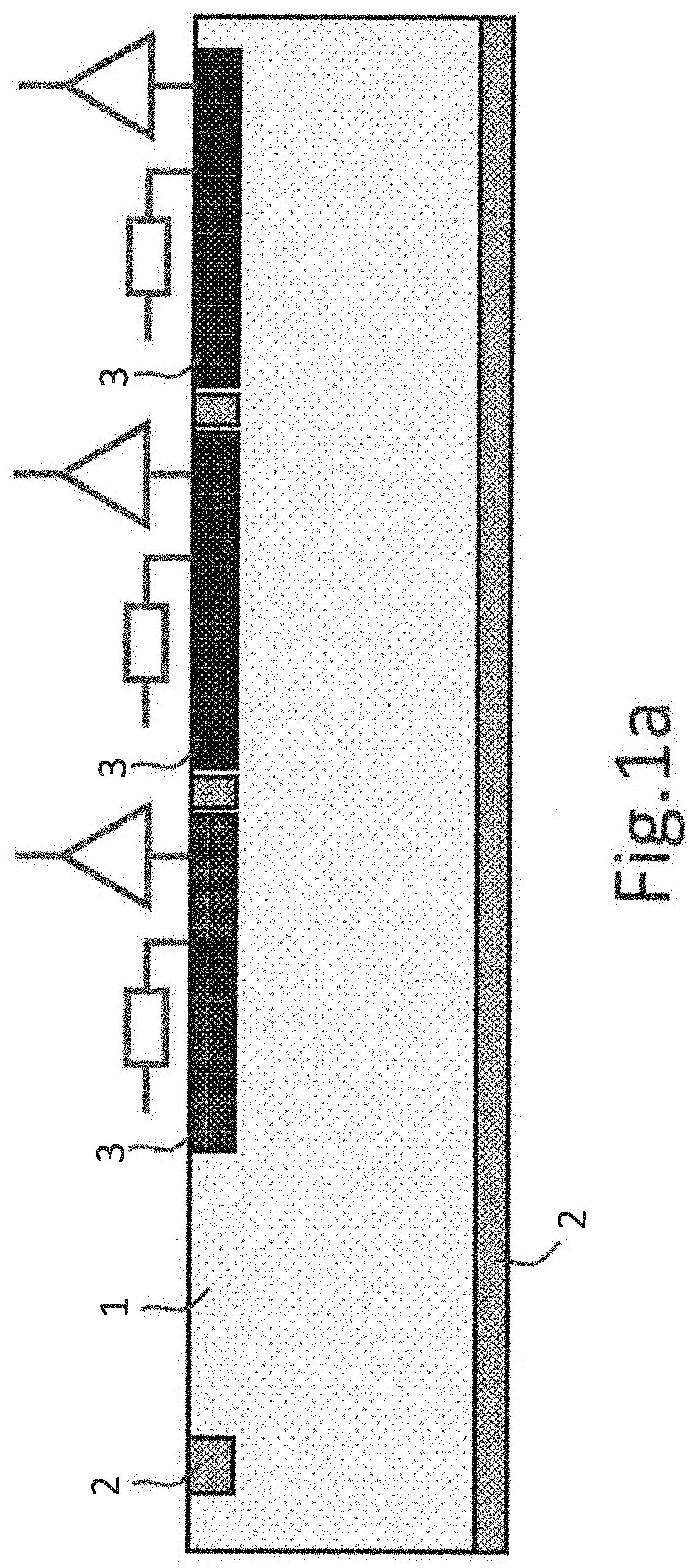
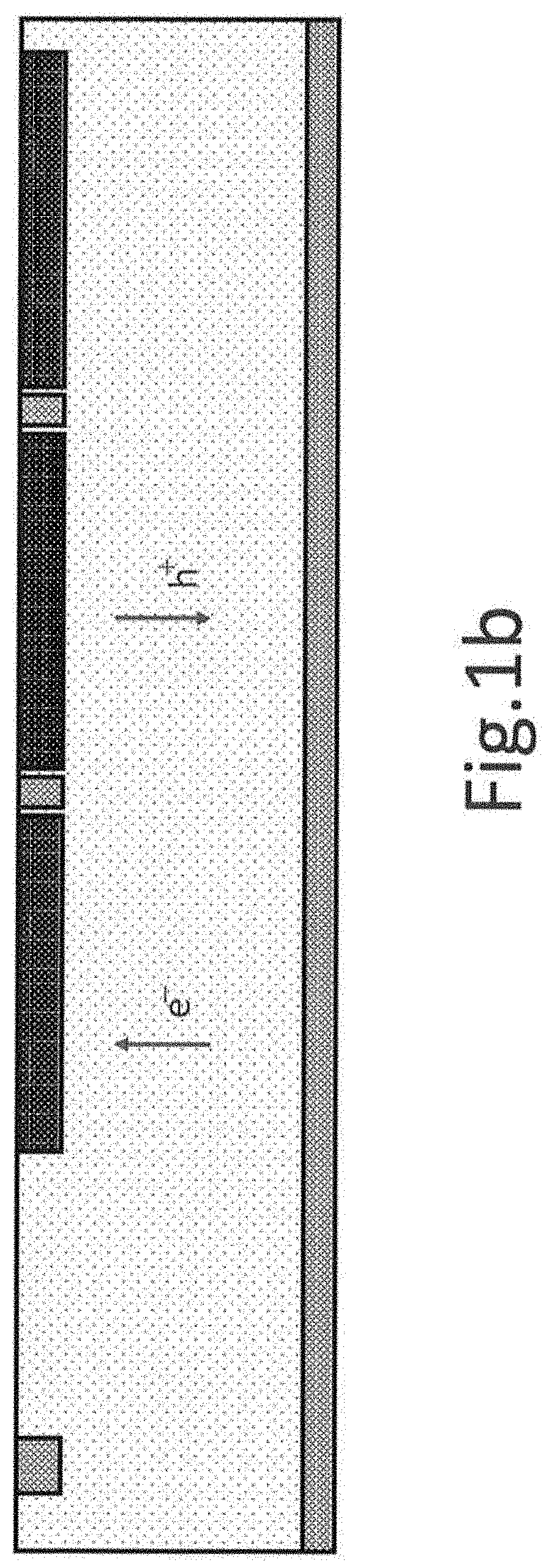
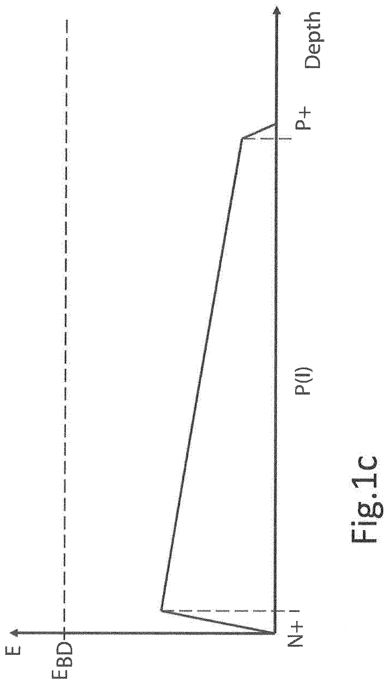
[0054]The sensor structure, which is not a diode, is composed by a lightly p-doped silicon substrate 1, n+ pixels 2 on the top surface and p+ uniform 3 doping on the backside. An additional n-doped, uniform layer 4 is present on the backside, deeper in the bulk than the p+ implant 3, in order to generate a gain region. Therefore, the doping structure of the sensor, from top to bottom, is NPNP. Between the pixel and the gain layer is provided a drift region 6. The inter-pixel p+ implant 7 is optional.

[0055]With this structure, the detector presents the n+ pixels 2 and p+ uniform doped region 3 as end terminals of the current such that upon detection the current signal ge...


PUM


Abstract

The present relates to a multi-junction photon detector comprising a semiconductor substrate, a plurality of n+ pixels on the top surface and a p+ uniform doping implant on the backside and at least one n-doped layer on the backside, deeper in the substrate bulk than the p+ implant, such that the detector presents a first PN junction corresponding to a drift and signal induction region and comprising the pixels on the substrate, and a second PN junction corresponding to a gain region and comprising the n-doped layer disposed on the backside of the detector active area deeper in the substrate bulk. These two junctions are operated in inverse polarization. The area between them contains a PN junction in direct polarization and it is fully depleted from the free charges.

Description

TECHNICAL FIELD[0001]The present invention relates to photon detector and more particularly to a high sensitivity single photon detector.BACKGROUND OF THE ART[0002]Existing semiconductors sensors comprise silicon p-substrate devices, which are the most common ones and which are possible to integrate with conventional microelectronic processes.[0003]The simplest silicon detectors comprise PIN diodes and are called pixel sensors. This type of sensor is represented in FIGS. 1A-1C. It comprises a P region 1 (bulk), P+ regions 2 and N+ regions 3 acting as pixels. As shown in FIG. 1A, it is composed by an N-on-P diode matrix, but P-on-N or alternative solutions are also possible.[0004]With this type of sensors, the bulk 1 of the sensor is depleted upon operation (detection). FIG. 1B shows that upon operation, the primary electrons e− produced in the depletion region (bulk) drift to the anode, whereas the holes h+ drift to the cathode, thereby inducing a signal.[0005]In these sensors, the ...

Claims


Application Information

Patent Timeline
IPC IPC(8): H01L31/107H01L31/02
CPCH01L31/1075H01L31/02027H01L27/1446
Inventor IACOBUCCI, GIUSEPPEVALERIO, PIERPAOLOPAOLOZZI, LORENZO
Owner UNIVERSITY OF GENEVA
Why Eureka
Try Eureka