Semiconductor structure and method for forming same

Active Publication Date: 2021-10-21
SEMICON MFG INT (SHANGHAI) CORP +1
View PDF0 Cites 0 Cited by
  • Summary
  • Abstract
  • Description
  • Claims
  • Application Information

AI Technical Summary

Benefits of technology

The present invention provides a semiconductor structure with better electrical performance by using different materials for different channel regions. This allows for the optimization of the semiconductor structure's performance.

Problems solved by technology

With the rapid development of semiconductor manufacturing technologies, semiconductor devices develop has trended toward higher element density and higher integration, and a developing trend of semiconductor process nodes according to the Moore's Law continuously weakens.

Method used


Image

  • Semiconductor structure and method for forming same
  • Semiconductor structure and method for forming same
  • Semiconductor structure and method for forming same

Examples


Embodiment Construction

[0014]It may be learned from the background art that currently formed semiconductor structures still have poor performance. The reason why the semiconductor structures have poor performance is now analyzed in combination with a method for forming a semiconductor structure.

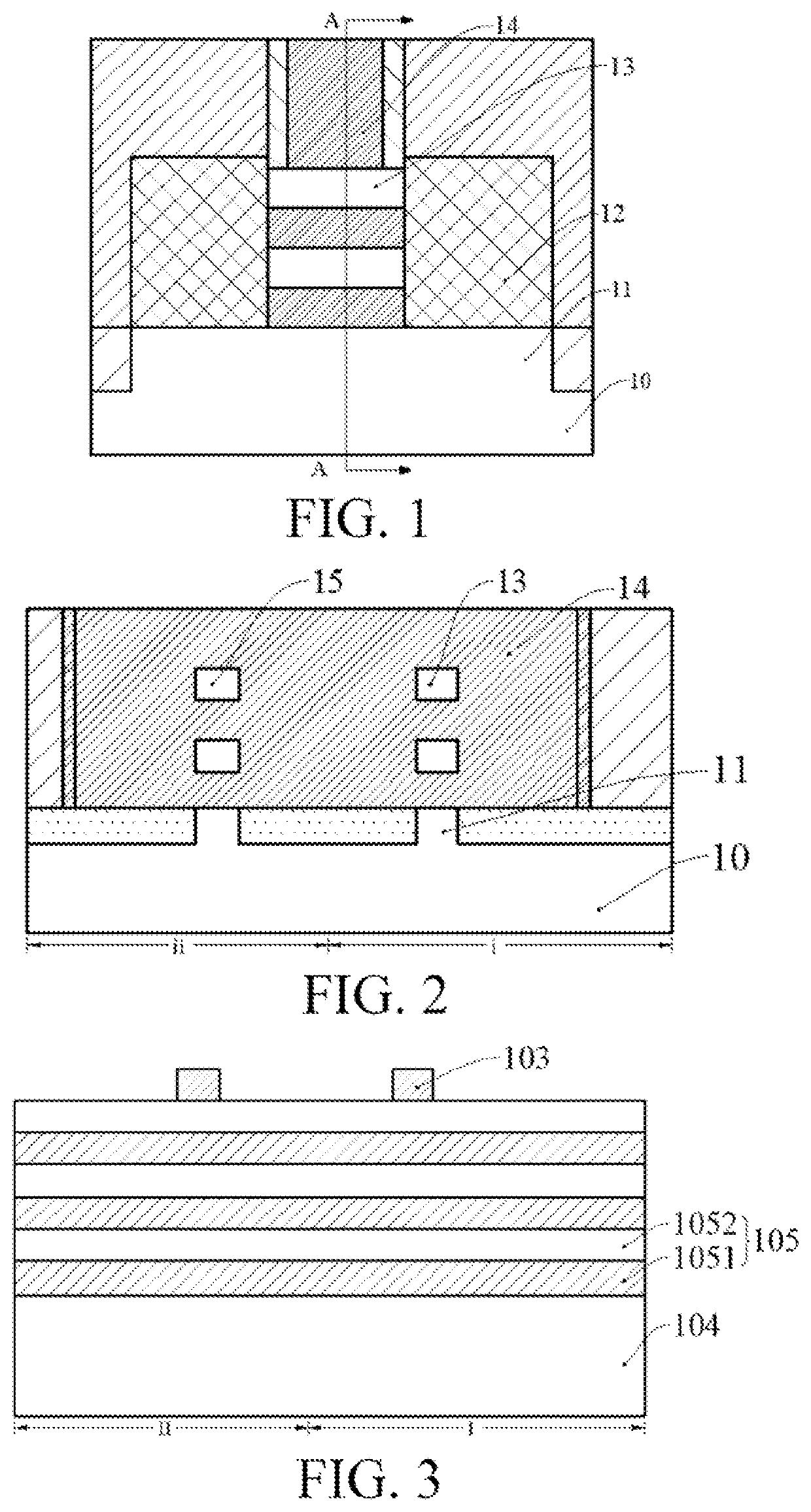
[0015]Referring to FIG. 1 and FIG. 2, FIG. 2 is a cross-sectional view of FIG. 1 in a direction AA, which is a schematic structural view of a semiconductor structure.

[0016]The semiconductor structure includes: a substrate 10 including a first region i and a second region 11; a plurality of discrete fins 11 located on the substrate 10; discrete first source-drain doped layers 12 on the fin 11 in the first region i; discrete second source-drain doped layers (not shown) on the fin 11 in the second region ii; one or more first channel layers 13 separated from each other and suspended above the fin 11 in the first region i, the first channel layers 13 being located between the first source-drain doped layers 12 and bein...


PUM


Abstract

A semiconductor structure and a method for forming same are provided. One form of the forming method includes: providing a base, the base including: a substrate and a channel stack on the substrate, the channel stack including a first channel layer and a second channel layer located on the first channel layer, the first channel layer and the second channel layer being made of different materials, and a first region and a second region, where the channel stack is located in the first region and the second region; forming an interlayer dielectric layer on the substrate exposed from the channel stack, where a gate opening from which the channel stack is exposed is formed in the interlayer dielectric layer; removing the second channel layer of the first region in the gate opening; removing the first channel layer of the second region in the gate opening; and forming a gate structure surrounding a remainder of the first channel layer and the second channel layer. In some implementations of the present disclosure, channel regions of transistors in the first region and the second region are made of different materials to meet performance requirements of different transistors, thereby optimizing electrical performance of the semiconductor structure.

Description

RELATED APPLICATIONS[0001]The present application claims priority to Chinese Patent Appln. No. 202010305031.3, filed Apr. 17, 2020, the entire disclosure of which is hereby incorporated by reference.BACKGROUNDTechnical Field[0002]The present disclosure relates to the field of semiconductor manufacturing, and in particular, to a semiconductor structure and a method for forming same.Related Art[0003]With the rapid development of semiconductor manufacturing technologies, semiconductor devices develop has trended toward higher element density and higher integration, and a developing trend of semiconductor process nodes according to the Moore's Law continuously weakens. Transistors are currently being widely used as the most basic semiconductor devices. Therefore, as the element density and integration of the semiconductor devices increase, channel lengths of the transistors need to be continuously shortened to adapt to reduced process nodes.[0004]In order to better meet a requirement of...

Claims


Application Information

Patent Timeline
IPC IPC(8): H01L21/8238H01L27/092H01L27/12H01L21/84
CPCH01L21/823807H01L21/84H01L27/1203H01L27/092H01L21/823821H01L27/0924H01L21/823828H01L29/78696H01L29/42392
Inventor ZHOU, FEI
Owner SEMICON MFG INT (SHANGHAI) CORP
Why Eureka
Try Eureka