Method of manufacturing semiconductor device
- Summary
- Abstract
- Description
- Claims
- Application Information
AI Technical Summary
Benefits of technology
Problems solved by technology
Method used
Image

Examples
Embodiment Construction
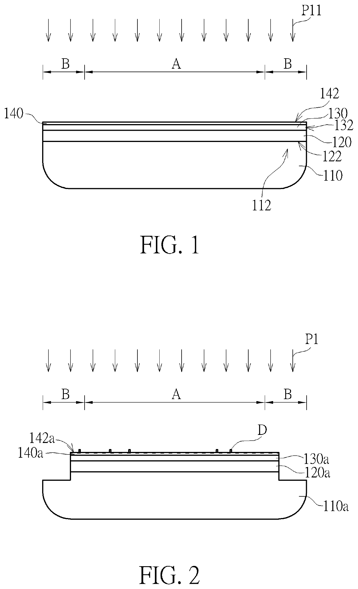
[0013]FIGS. 1-6 schematically depict cross-sectional views of a method of manufacturing a semiconductor device according to an embodiment of the present invention. As shown in FIG. 1, a device wafer 110 is provided. The device wafer 110 may be divided into a product-obtaining part A and an edge part B, wherein the edge part B surrounds the product-obtaining part A. The product-obtaining part A may include transistors with various functions, and an inter-dielectric layer may cover these transistors. A device layer 120 may be formed to cover the device wafer 110. The device layer 120 may include inter-metal dielectric layers such as metal 0 to metal 4 layers, depending upon practical requirements. A passivation layer 130 is formed to cover the device layer 120. Preferably, the passivation layer 130 may include a silicon nitride layer, but it is not limited thereto. Still preferably, the passivation layer 130 may include a UV silicon nitride layer, but it is not limited thereto.
[0014]I...
PUM
 Abstract
Description
Claims
Application Information
 - R&D Engineer
- R&D Manager
- IP Professional
- Industry Leading Data Capabilities
- Powerful AI technology
- Patent DNA Extraction
Browse by: Latest US Patents, China's latest patents, Technical Efficacy Thesaurus, Application Domain, Technology Topic.
© 2024 PatSnap. All rights reserved.Legal|Privacy policy|Modern Slavery Act Transparency Statement|Sitemap