Eureka AIR delivers breakthrough ideas for toughest innovation challenges, trusted by R&D personnel around the world.

Method for measuring chips bonding strength and chips bonding auxiliary structure

Active Publication Date: 2021-11-18
UNITED MICROELECTRONICS CORP
View PDF2 Cites 0 Cited by
  • Summary
  • Abstract
  • Description
  • Claims
  • Application Information

AI Technical Summary

Benefits of technology

The present patent provides a method and structure for measuring the strength of chips that are bonded together. This is achieved by creating a pattern on one of the chips, which results in a space around the pattern when the other chip is bonded. The dimensions of the pattern and the space can be measured using non-destructive methods, which allows the strength of the bond to be estimated based on the dimensions and the elastic modulus of the chips. This method reduces manufacturing costs by not damaging the bonded structure and improves accuracy by eliminating operator-related measuring variations.

Problems solved by technology

Insufficient bonding strength may cause a risk of chip peeling and cracking during processing, resulting in device failure.
Although this method requires relatively simple instruments and equipment, but it is still a destructive detection method.
Furthermore, due to the brittle nature of the semiconductor chips, the step of inserting the blade into the bonded semiconductor chips requires operation of trained and experienced staff.
The measured value may vary depending on the operator, and this may result in considerable measurement error.

Method used


Image

  • Method for measuring chips bonding strength and chips bonding auxiliary structure
  • Method for measuring chips bonding strength and chips bonding auxiliary structure
  • Method for measuring chips bonding strength and chips bonding auxiliary structure

Examples


Embodiment Construction

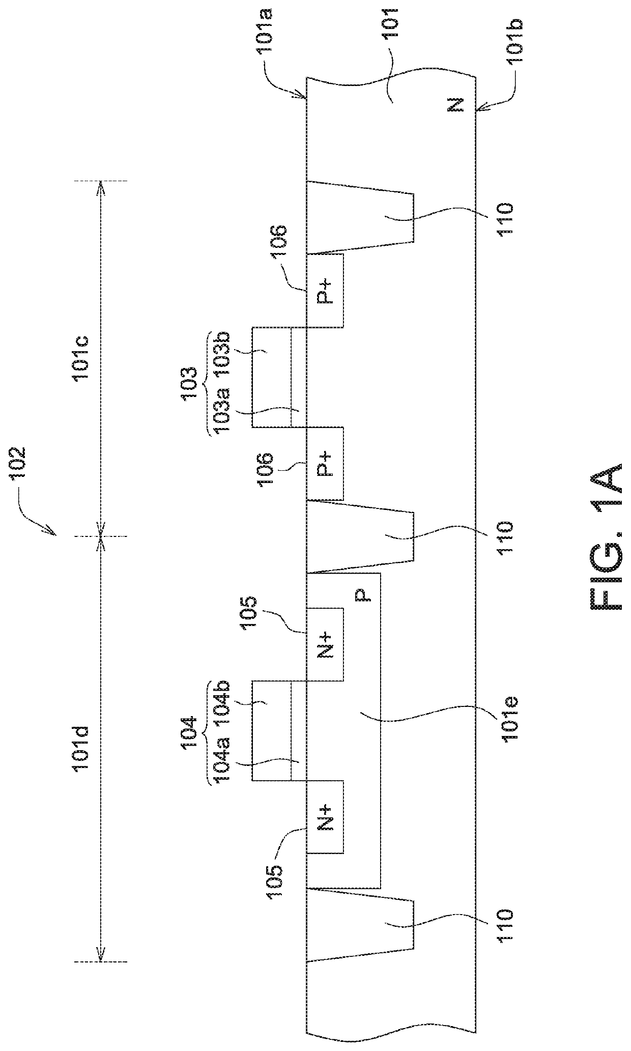
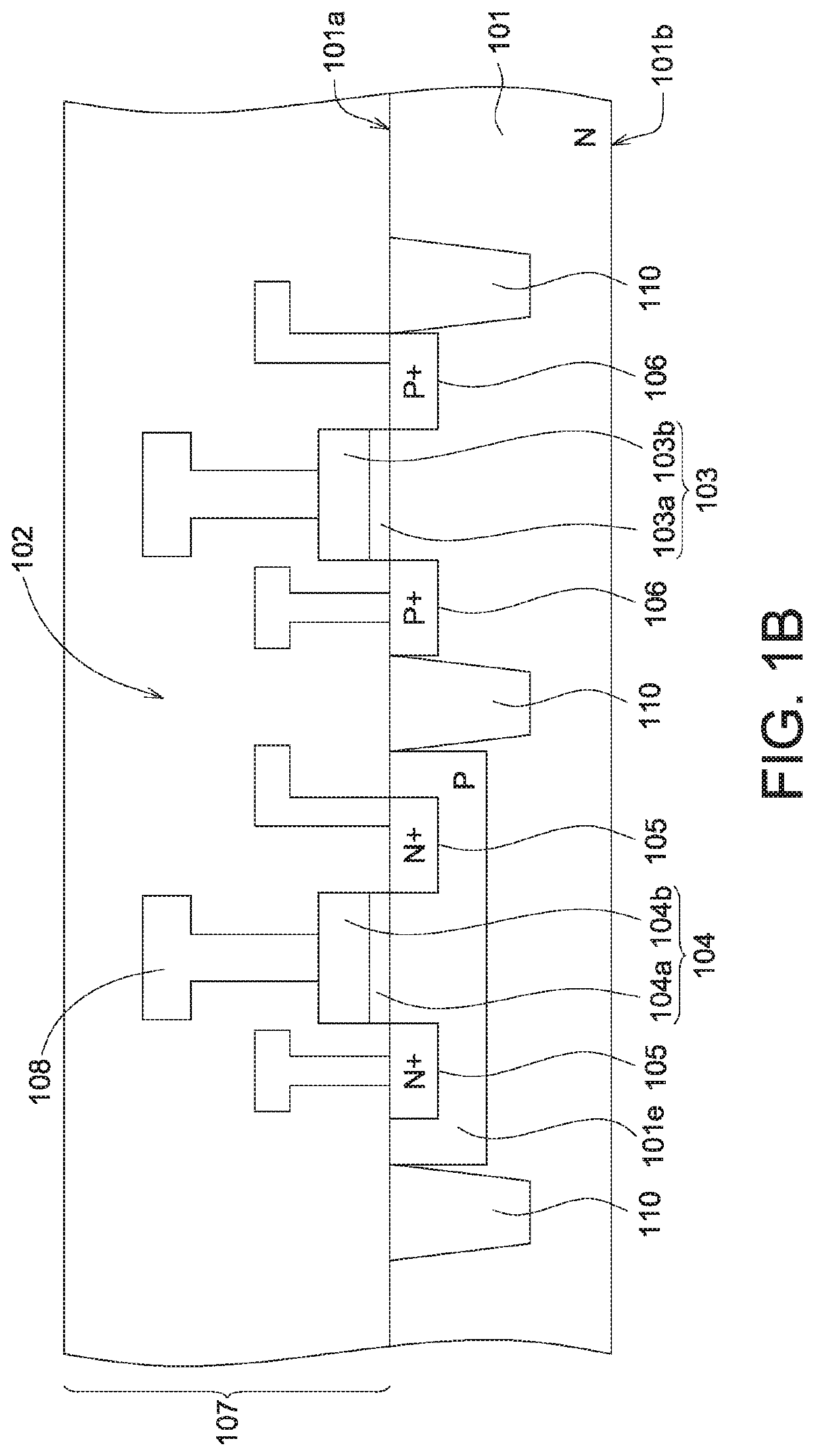
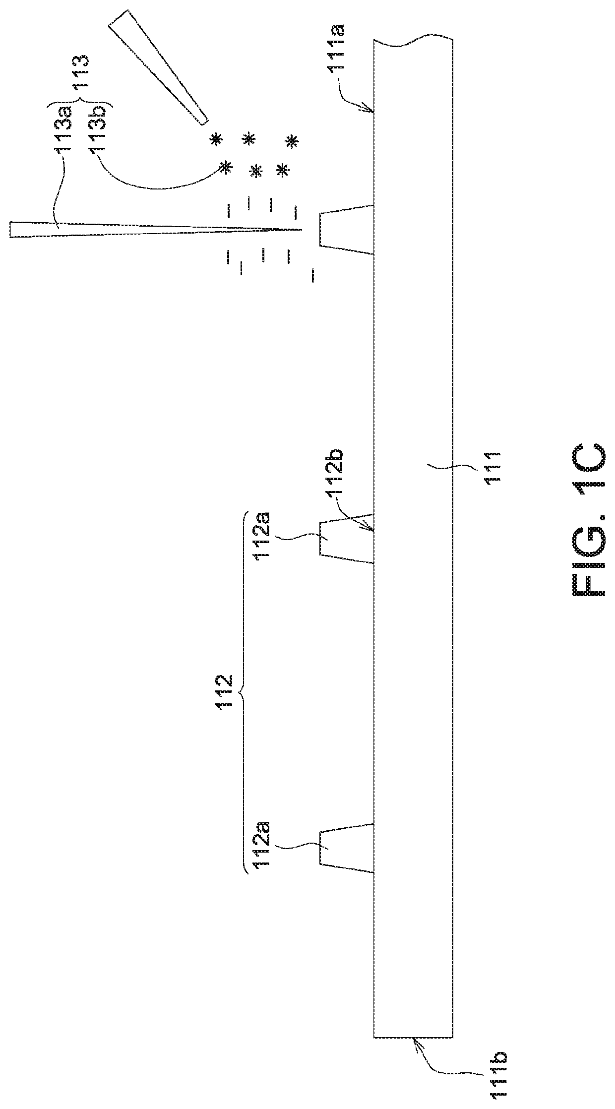
[0014]The embodiments as illustrated below provide a method for measuring chip bonding strength and a chips bonding auxiliary structure, which can achieve the purpose of reducing the manufacture cost, eliminating the measuring variation due to human operation, and improving the measurement accuracy. The present disclosure will now be described more specifically with reference to the following embodiments illustrating the structure and arrangements thereof.

[0015]It is to be noted that the following descriptions of preferred embodiments of this disclosure are presented herein for purpose of illustration and description only. It is not intended to be exhaustive or to be limited to the precise form disclosed. Also, it is important to point out that there may be other features, elements, steps, and parameters for implementing the embodiments of the present disclosure which are not specifically illustrated. Thus, the descriptions and the drawings are to be regard as an illustrative sense ...


PUM


Abstract

A method for measuring chips bonding strength includes steps as follows: An auxiliary pattern is formed on a first surface of a first chip. A second surface of a second chip is bonded to the first surface to form at least one gap space surrounding the auxiliary pattern. Next, dimensions of the at least one gap space and the auxiliary pattern are measure respectively; and the bonding strength between the first chip and the second chip is estimated according to the dimensions.

Description

[0001]This application claims the benefit of People's Republic of China application Serial No. 202010396124.1 filed May 12, 2020, the subject matter of which is incorporated herein by reference.BACKGROUNDTechnical Field[0002]The disclosure relates to a method for fabrication semiconductor devices and the auxiliary structure thereof, and more particularly to a method for measuring the bonding strength of semiconductor chips and a chips bonding auxiliary structure.Description of Background[0003]Chip bonding technology refers to a method by which two semiconductor chips (for example, wafers) are cleaned and bonded together, and then subjected to a high temperature annealing treatment to form a chemical bond connection at the interface of these two semiconductor chips, has been widely used in the manufacturing process of semiconductor circuits (including substrate engineering, integrated circuit wiring, micro-electromechanical system (MEMS) and packaging technologies), and has become an...

Claims


Application Information

Patent Timeline
IPC IPC(8): H01L21/66
CPCH01L22/12H01L22/30H01L22/20H01L23/544G01N19/04H01L2223/544
Inventor ZHANG, SHENGPANG, CHIEN-KEEZHAO, XIN
Owner UNITED MICROELECTRONICS CORP
Why Eureka
Eureka Blog
Learn More