
Apparatus and method with in-memory processing

a technology of in-memory processing and apparatus, applied in the field of apparatus and methods with in-memory processing, can solve the problems of inefficient performance and miniaturization, large amount of computation required for complex input data, and large amount of memory access frequency of processing devices

Active Publication Date: 2021-11-25
SAMSUNG ELECTRONICS CO LTD
View PDF5 Cites 10 Cited by
  • Summary
  • Abstract
  • Description
  • Claims
  • Application Information

AI Technical Summary

Benefits of technology

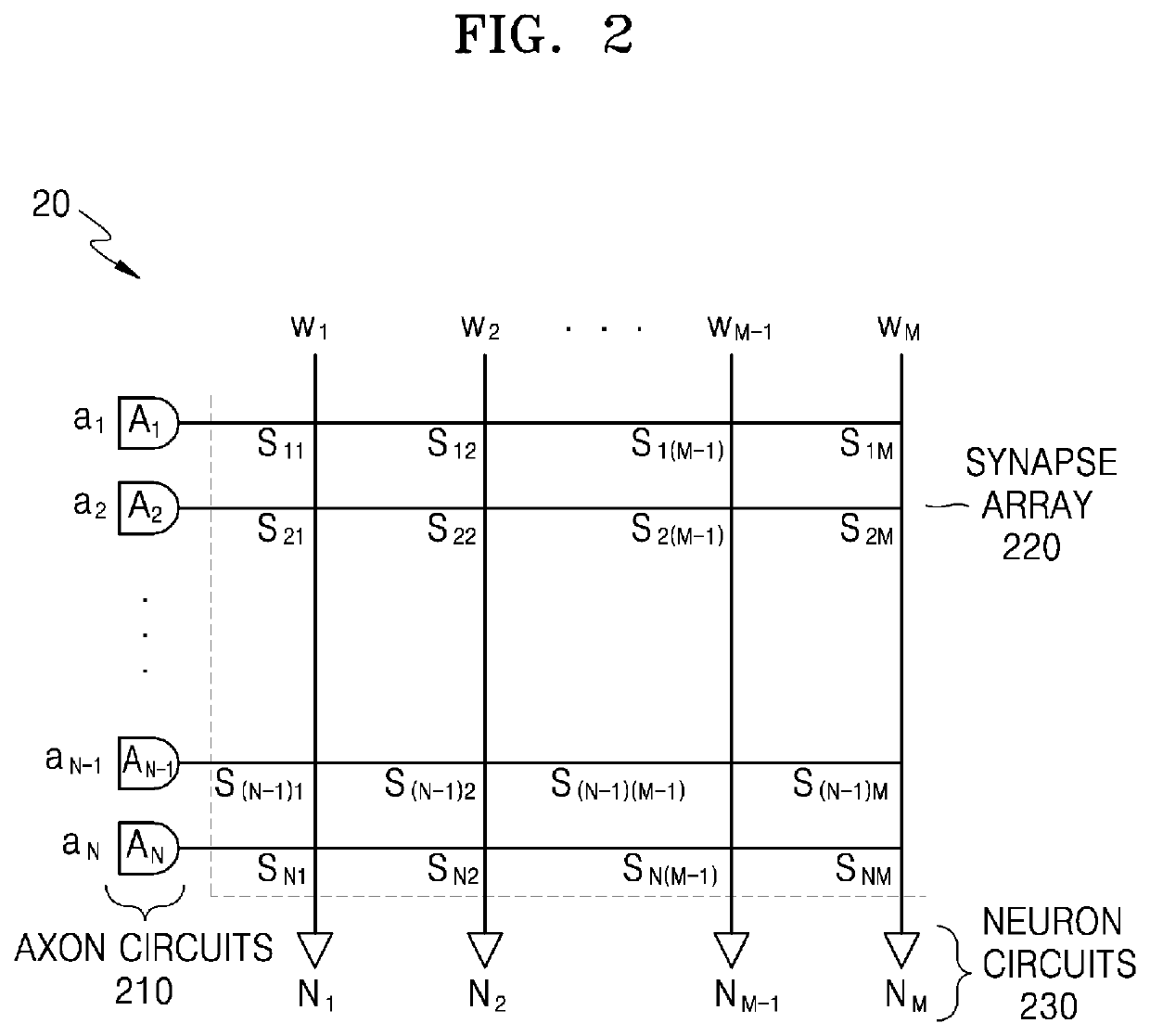
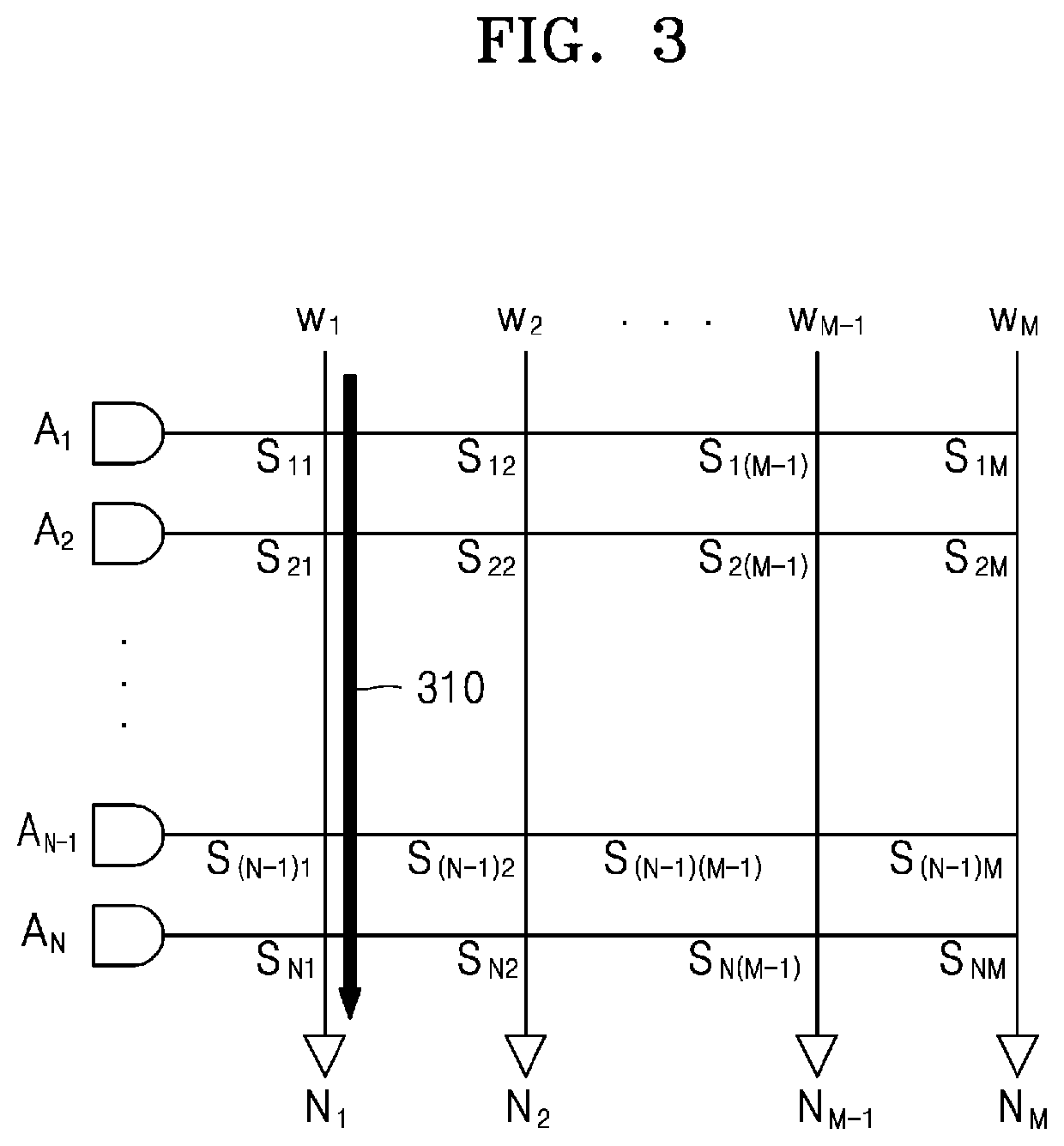
The patent describes an apparatus and method for performing in-memory processing. The apparatus includes a memory cell array, a sampling circuit, and a processing circuit. The memory cell array outputs a current sum of a column current based on an input signal applied to row lines. The sampling circuit charges a capacitor connected to each column line using a sampling voltage corresponding to the current sum. The processing circuit compares a reference voltage and the currently charged voltage in the capacitor and determines the quantization level by performing time-digital conversion when the currently charged voltage reaches the reference voltage. The technical effects of this invention include improved processing speed, reduced latency, and improved accuracy.

Problems solved by technology

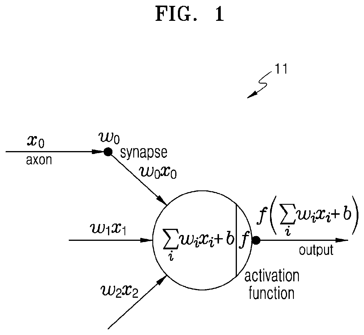
Neural network processing requires a large amount of computation for complex input data.
As neural network data increases and connectivity of the architecture forming a neural network gets complicated, the computational amount and memory access frequency of the processing device may excessively increase, resulting in inefficient performance and miniaturization issues.

Method used


Image

  • Apparatus and method with in-memory processing
  • Apparatus and method with in-memory processing
  • Apparatus and method with in-memory processing

Examples


Embodiment Construction

[0045]The following detailed description is provided to assist the reader in gaining a comprehensive understanding of the methods, apparatuses, and / or systems described herein. However, various changes, modifications, and equivalents of the methods, apparatuses, and / or systems described herein will be apparent after an understanding of the disclosure of this application. For example, the sequences of operations described herein are merely examples, and are not limited to those set forth herein, but may be changed as will be apparent after an understanding of the disclosure of this application, with the exception of operations necessarily occurring in a certain order. Also, descriptions of features that are known after understanding of the disclosure of this application may be omitted for increased clarity and conciseness.

[0046]The features described herein may be embodied in different forms, and are not to be construed as being limited to the examples described herein. Rather, the e...


PUM


Abstract

An apparatus for performing in-memory processing includes a memory cell array of memory cells configured to output a current sum of a column current flowing in respective column lines of the memory cell array based on an input signal applied to row lines of the memory cells, a sampling circuit, comprising a capacitor connected to each of the column lines, configured to be charged by a sampling voltage of a corresponding current sum of the column lines, and a processing circuit configured to compare a reference voltage and a currently charged voltage in the capacitor in response to a trigger pulse generated at a timing corresponding to a quantization level, among quantization levels, time-sectioned based on a charge time of the capacitor, and determine the quantization level corresponding to the sampling voltage by performing time-digital conversion when the currently charged voltage reaches the reference voltage.

Description

CROSS-REFERENCE TO RELATED APPLICATION[0001]This application claims the benefit under 35 USC 119(a) of Korean Patent Application No. 10-2020-0061746, filed on May 22, 2020, in the Korean Intellectual Property Office, the entire disclosure of which is incorporated herein by reference for all purposes.BACKGROUND1. Field[0002]The disclosure relates to an apparatus and method with in-memory processing.2. Description of Related Art[0003]A neural network is a computing system implemented on the basis of a computational architecture. Neural network processing requires a large amount of computation for complex input data. As neural network data increases and connectivity of the architecture forming a neural network gets complicated, the computational amount and memory access frequency of the processing device may excessively increase, resulting in inefficient performance and miniaturization issues. For example, neural network processing may include a multiply-accumulate (MAC) operation that...

Claims


Application Information

Patent Timeline
Patent Type & Authority Applications(United States)
IPC IPC(8): G11C13/00
CPCG11C13/0069G11C13/0038G11C13/0028G11C13/0061G11C13/0026G11C13/004G11C5/063G11C5/10G11C5/147G11C11/54G11C13/0007G11C7/1006G06N3/063
Inventor LEE, HYUNGWOOKIM, SANGJOONJU, YONGMIN
Owner SAMSUNG ELECTRONICS CO LTD
Learn More