Semiconductor device

a technology of semiconductor devices and semiconductors, applied in the direction of pulse techniques, basic electric elements, electronic switching, etc., can solve the problems of parasitic oscillations and the complication of a semiconductor device configuration, and achieve the effect of suppressing parasitic oscillations and simple configuration

Pending Publication Date: 2021-11-25
MITSUBISHI ELECTRIC CORP
View PDF14 Cites 0 Cited by
  • Summary
  • Abstract
  • Description
  • Claims
  • Application Information

AI Technical Summary

Benefits of technology

[0004]The present disclosure has been conceived to solve a problem as described above, and it is an object of the present disclosure to provide a semiconductor de

Problems solved by technology

In the semiconductor device, positive feedback circuits are sometimes formed by parasitic capacitance and stray inductance of the semicondu

Method used


Image

  • Semiconductor device
  • Semiconductor device
  • Semiconductor device

Examples


embodiment 1

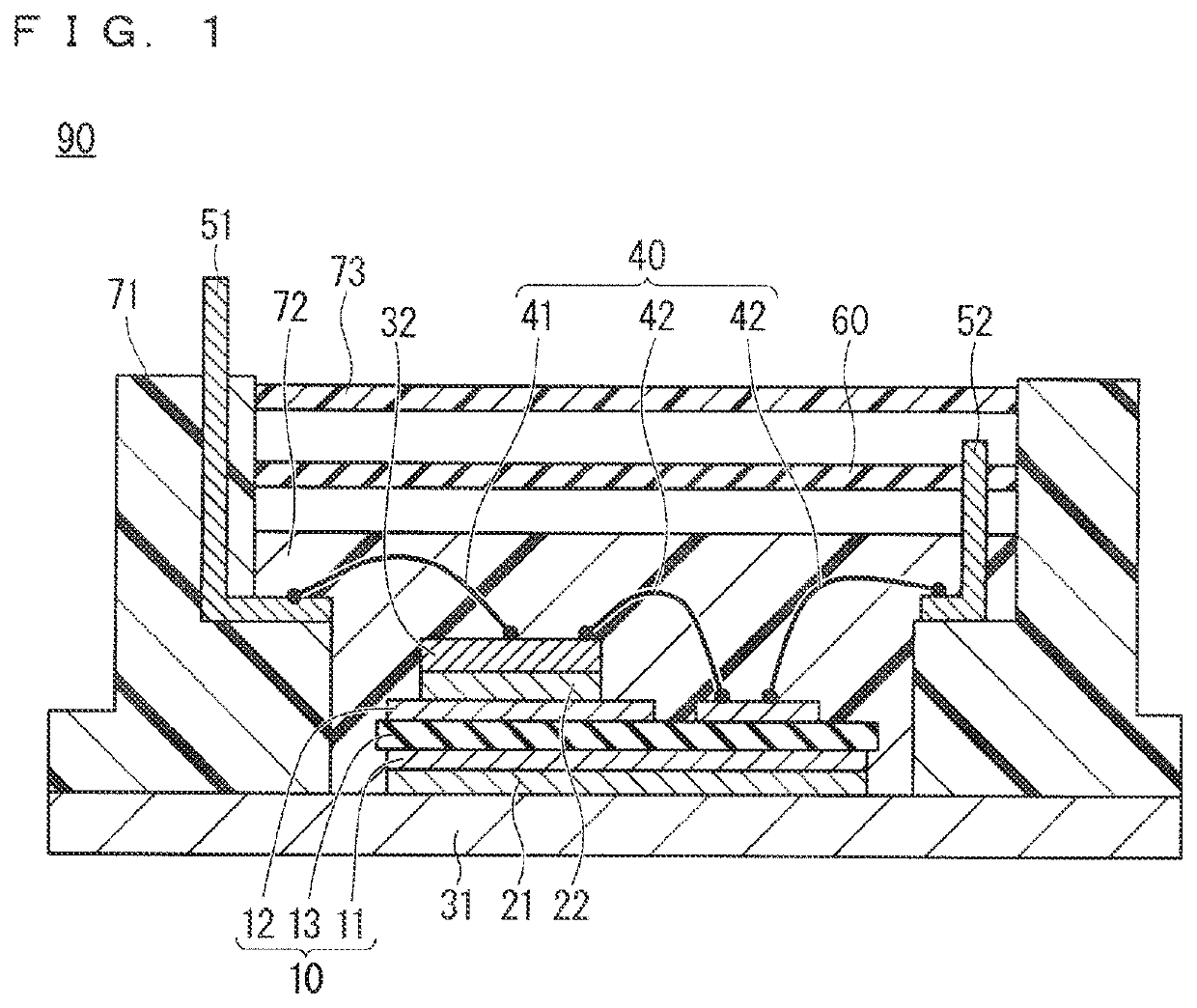
[0016]FIG. 1 is a cross-sectional view illustrating an example of a configuration of a semiconductor device 90 in Embodiment 1. The semiconductor device 90 includes an insulating substrate 10 (a first substrate), a solder joint 21, a solder joint 22, a base plate 31, at least one semiconductor chip 32 (semiconductor component), a plurality of wires 40, a plurality of main electrodes 51, a drive electrode 52, a printed circuit board 60 (second substrate), a case 71, a sealing material 72, and a lid 73. The insulating substrate 10 includes an insulating plate 13 having a first surface (a lower surface in FIG. 1) and a second surface (an upper surface in FIG. 1), a conductor layer 11 located on the first surface, and a conductor layer 12 located on the second surface and having a pattern. The plurality of wires 40 include a main wire 41 and drive wires 42.

[0017]The case 71 has a space to be closed by the case 71 being combined with the base plate 31 and the lid 73, and the other member...

embodiment 2

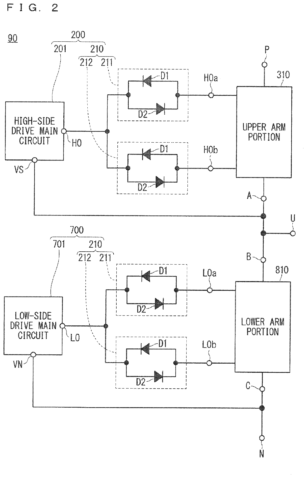
[0032]Referring to FIG. 5, a semiconductor device in Embodiment 2 includes a plurality of inserted circuits 220 in place of the plurality of inserted circuits 210 (FIG. 3: Embodiment 1). Each of the plurality of inserted circuits 220, that is, each of a first inserted circuit 221 and a second inserted circuit 222 includes a first resistive element R1 connected in series with the first diode D1 and connected in parallel with the second diode D2, and includes a second resistive element R2 connected in series with the second diode D2 and connected in parallel with the first diode D1. The other configuration is substantially the same as the above-mentioned configuration in Embodiment 1, so that the same or similar components bear the same reference signs, and description thereof will be not repeated.

[0033]According to the present embodiment, when ja current caused due to parasitic oscillations flows because it is not completely interrupted by the first diode D1 and the second diode D2, ...

embodiment 3

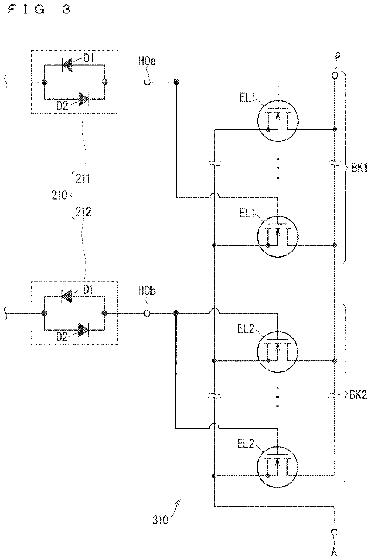
[0035]Referring to FIG. 6, a semiconductor device in Embodiment 3 includes an upper arm portion 320 in place of the upper arm portion 310 (FIG. 5: Embodiment 2). In the upper arm portion 320, a gate resistive element RG is interposed between each of the inserted circuits 220 of the drive circuit and each of the plurality of semiconductor elements EL. Although not shown, the gate resistive element RG is similarly interposed in the lower arm portion. The gate resistive element RG may be a resistive element built in the semiconductor chip 32 in which the semiconductor elements EL are formed, or may be a resistive element added separately from the semiconductor chip.

[0036]According to the present embodiment, the plurality of first semiconductor elements EL1 are separated from one another by gate resistive dements RG, and also the plurality of second semiconductor elements EL2 are separated from one another by gate resistive elements RG. Parasitic oscillations are thus less likely to occ...


PUM


Abstract

A plurality of semiconductor elements connected in parallel with one another include a plurality of first semiconductor elements and a plurality of second semiconductor elements. A drive circuit to provide a gate signal to each of the plurality of semiconductor elements EL includes a main circuit and a plurality of inserted circuits including a first inserted circuit and a second inserted circuit. The first inserted circuit is inserted between the main circuit and the plurality of first semiconductor dements. The second inserted circuit is inserted between the main circuit and the plurality of second semiconductor elements. Each of the first inserted circuit and the second inserted circuit includes a first diode having a forward direction toward the main circuit and a second diode connected in anti-parallel with the first diode.

Description

BACKGROUND OF THE INVENTIONField of the Invention[0001]The present disclosure relates to semiconductor devices and, in particular, to a semiconductor device including a plurality of semiconductor elements connected in parallel with one another.Description of the Background Art[0002]A power semiconductor device includes semiconductor elements as switching elements in many cases. For example, semiconductor dements each having a gate electrode, such as metal oxide semiconductor field effect transistors (MOSFETs) and insulated gate bipolar transistors (IGBTs), are used. In particular, a high power semiconductor device often includes switching elements connected in parallel with one another. In the semiconductor device, positive feedback circuits are sometimes formed by parasitic capacitance and stray inductance of the semiconductor elements to result in occurrence of parasitic oscillations. The severity of parasitic oscillations is likely to increase in proportion to the number of semic...

Claims


Application Information

Patent Timeline
IPC IPC(8): H01L25/16H01L29/16H01L23/053H01L23/498
CPCH01L25/165H01L29/1608H01L24/48H01L23/49822H01L23/053H02M1/088H03K17/161H03K17/687H01L2224/73265H01L2224/48091H01L2924/181H01L2224/48227H01L2924/19107H01L2224/48464H01L2224/48157H01L2924/10272H02M7/5387H01L2224/32238H01L2224/32225H01L2224/291H01L2924/00014H01L2924/00012H01L2924/00H01L2924/014
Inventor MASUDA, AKIYOSHIMIYAZAKI, YUJI
Owner MITSUBISHI ELECTRIC CORP
Why Eureka
Try Eureka