Electronic device

Pending Publication Date: 2021-12-23
E INK HLDG INC
View PDF0 Cites 0 Cited by
  • Summary
  • Abstract
  • Description
  • Claims
  • Application Information

AI Technical Summary

Benefits of technology

The patent text describes a method to improve the bonding stability between conductive particles and a flexible substrate in an anisotropic conductive film. This is achieved by adding protrusions on the bonding pad of the flexible substrate, which increases the contact area between the conductive particles and enhances the stability of the bond. Additionally, the insulation layers on the conductive particles may be easier to break with the protrusions, reducing the external force required for effective contact and preventing the bonding pad of the flexible substrate from collapsing during the bonding process.

Problems solved by technology

For the electronic device that utilizes a flexible substrate, the bonding pad of the flexible substrate may collapse due to such greater bonding pressure.

Method used


Image

  • Electronic device
  • Electronic device
  • Electronic device

Examples


Embodiment Construction

[0037]Reference will now be made in detail to the present embodiments of the invention, examples of which are illustrated in the accompanying drawings. Wherever possible, the same reference numbers are used in the drawings and the description to refer to the same or like parts.

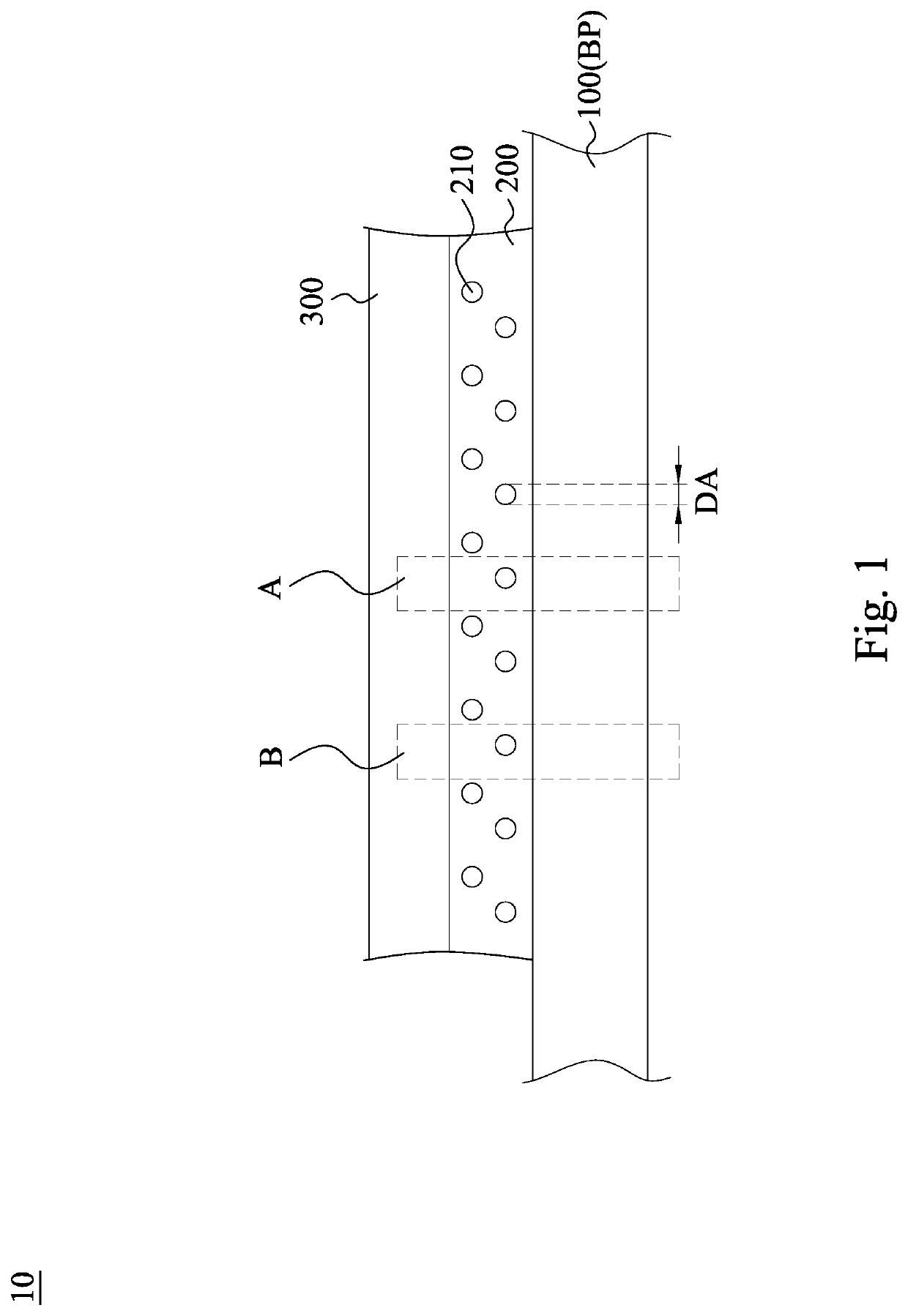
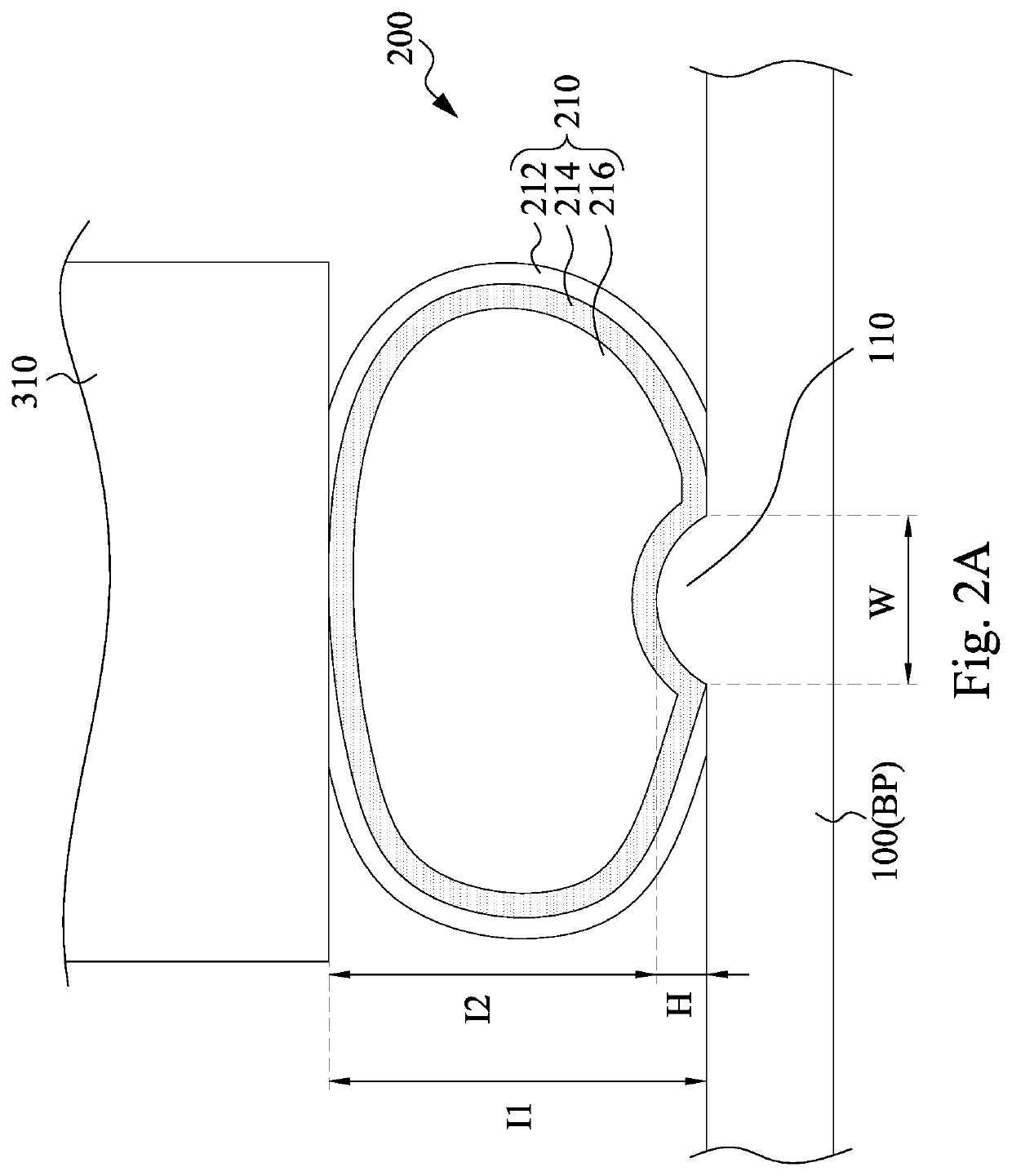
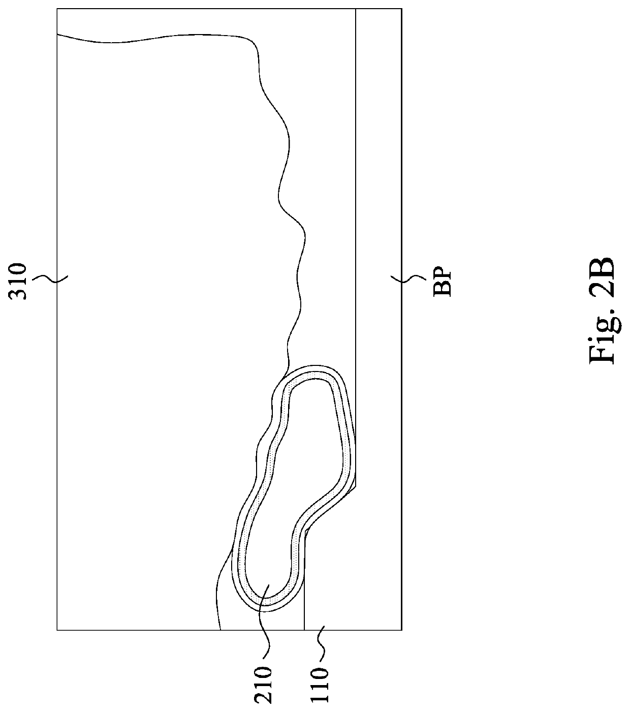
[0038]FIG. 1 is a cross-sectional view of an electronic device 10 according to one embodiment of the present disclosure. The electronic device 10 includes a flexible substrate 100, an anisotropic conductive film 200, and an electronic element 300. FIG. 2A is an enlarged view of the region A in FIG. 1. Reference is made to FIG. 1 and FIG. 2A. The flexible substrate 100 includes a bonding pad BP and protrusions 110 located on the bonding pad BP. The anisotropic conductive film 200 includes a plurality of conductive particles 210. The conductive particles 210 are in contact with the protrusions 110. The anisotropic conductive film 200 is located between the bonding pad BP of the flexible substrate 100 and the ele...


PUM


Abstract

An electronic device includes a flexible substrate, an anisotropic conductive film, and an electronic element. The flexible substrate includes an active area, a bonding pad, and a plurality of protrusions located on the bonding pad. The anisotropic conductive film includes a plurality of conductive particles. The conductive particles are in contact with the protrusions. The anisotropic conductive film is located between the bonding pad of the flexible substrate and the electronic element.

Description

CROSS-REFERENCE TO RELATED APPLICATION[0001]This application claims priority to Taiwan Application Serial Number 109120900, filed Jun. 19, 2020, which is herein incorporated by reference in its entirety.BACKGROUNDField of Invention[0002]The present invention relates to an electronic device.Description of Related Art[0003]The bonding pad of an electronic device nowadays has a flat. In order to make the conductive particles of the anisotropic conductive film deform effectively and be in contact with the conductive layer of the bonding pad, the contact are between the conductive particles and the bonding pad must be large enough to reach the effective contact. Therefore, a greater bonding pressure is required to ensure that the effective contact can be formed between the conductive particles and the bonding pad. For the electronic device that utilizes a flexible substrate, the bonding pad of the flexible substrate may collapse due to such greater bonding pressure.[0004]Accordingly, it ...

Claims


Application Information

Patent Timeline
IPC IPC(8): H05K1/11H05K1/02H01L29/423
CPCH05K1/118H01L29/42364H05K1/0213H05K3/323H05K3/361H05K2201/0221H05K2201/0367H01L27/1218H01L27/1244
Inventor LIN, KUAN-YILU, CHUN-YU
Owner E INK HLDG INC
Why Eureka
Try Eureka