
Display panel, display substrate, and manufacturing method thereof

a technology of display substrate and substrate, applied in the field of display substrate, can solve the problems of insufficient light-shielding and non-uniformity of filled liquid crystals, difficult to completely control the shape and bottom size of bps materials, and low bottom absorbance, so as to achieve good light-shielding effect, excellent strength and flexibility, and good light-shielding properties

Active Publication Date: 2022-02-17
SHENZHEN CHINA STAR OPTOELECTRONICS TECH CO LTD
View PDF0 Cites 0 Cited by
  • Summary
  • Abstract
  • Description
  • Claims
  • Application Information

AI Technical Summary

Benefits of technology

[0005]The present disclosure provides a display panel, a display substrate, and a manufacturing method thereof, which can improve light-shielding effect of a BPS light-shielding layer in a display substrate and make liquid crystals in a display panel to be uniformly distributed. The technical problems of insufficient light-shielding and nonuniformity of filled liquid crystals caused by not easy to control shapes and bottom sizes of BPS materials in current technology can be solved.
[0040]Beneficial effect: the beneficial effect of the present disclosure is that the present disclosure provides a display panel, a display substrate, and a manufacturing method thereof; the display substrate comprises a substrate, a first planar layer disposed on one side of the substrate, and a BPS light-shielding layer disposed on one side surface of the first planar layer away from the substrate; wherein the BPS light-shielding layer is made of a composite material including polydopamine and graphene oxide. Because the composite material including polydopamine and graphene oxide has physical adhesion, excellent strength and flexibility, and good light-shielding properties, it can strengthen a binding force between the BPS light-shielding layer and the first planar layer and make the BPS light-shielding layer have better light-shielding effect. The manufacturing method of the display substrate is simple that can save costs of equipment and processes. It can make liquid crystals uniformly filled when the display substrate is used in a display panel, thereby improving display quality.

Problems solved by technology

Technical problem: bottom absorbance is less than top absorbance in current BPS materials of a display substrate.
In practical manufacturing processes, it is hard to completely control shapes and bottom sizes of BPS materials, thereby causing problems of insufficient light-shielding and nonuniformity of filled liquid crystals.

Method used


Image

  • Display panel, display substrate, and manufacturing method thereof
  • Display panel, display substrate, and manufacturing method thereof
  • Display panel, display substrate, and manufacturing method thereof

Examples


Embodiment Construction

[0046]The specific embodiments described with reference to the attached drawings are all exemplary and are intended to illustrate and interpret the present disclosure.

[0047]An embodiment of the present disclosure can solve the technical problems of insufficient light-shielding and nonuniformity of filled liquid crystals caused by bottom absorbance in current BPS materials of a display substrate being less than top absorbance, and shapes and bottom sizes of BPS materials being not easy to control.

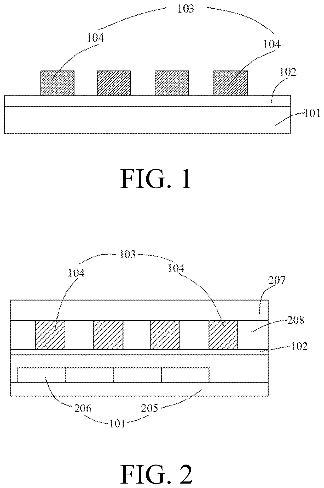
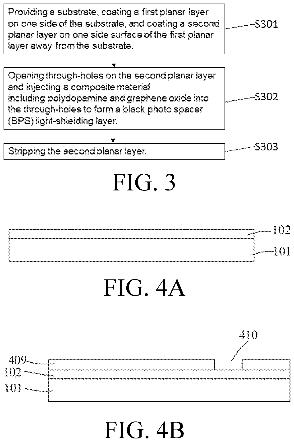
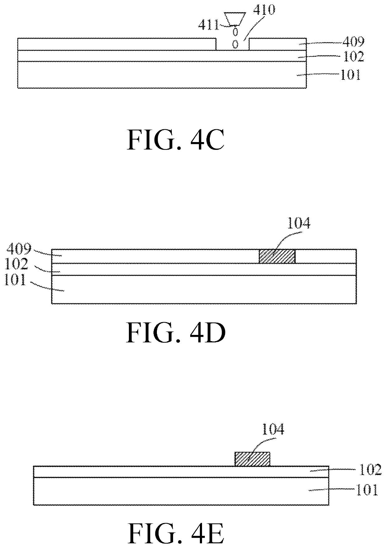
[0048]Referring to FIG. 1, a display substrate provided by the present disclosure comprises a substrate 101, a first planar layer 102 disposed on one side of the substrate 101, and a BPS light-shielding layer 103 disposed on one side surface of the first planar layer 102 away from the substrate 101; wherein the BPS light-shielding layer 103 is made of a composite material including polydopamine and graphene oxide.

[0049]The BPS light-shielding layer 103 comprises a plurality of matrix distrib...


PUM

PropertyMeasurementUnit
temperatureaaaaaaaaaa

Abstract

The present disclosure provides a display panel, a display substrate, and a manufacturing method thereof. The display substrate comprises a substrate, a first planar layer, and a BPS light-shielding layer. Wherein the BPS light-shielding layer is made of a composite material including polydopamine and graphene oxide, which can strengthen a binding force between the BPS light-shielding layer and the first planar layer and improve light-shielding effect of the BPS light-shielding layer. The manufacturing method of the display substrate is simple, and making liquid crystals uniformly filled, thereby improving display quality of panels.

Description

FIELD OF INVENTION[0001]The present disclosure relates to the field of display technologies, and more particularly, to a display panel, a display substrate, and a manufacturing method thereof.BACKGROUND OF INVENTION[0002]At present, a black photo spacer (BPS) light-shielding layer, in a display substrate of a liquid crystal display panel, is made of a new type of material, which has characteristics of conventional spacer materials, such as excellent elastic recovery and lower pollution to liquid crystals, and has characteristics of black matrix materials, such as a higher optical density (OD) value to shielding light.[0003]Technical problem: bottom absorbance is less than top absorbance in current BPS materials of a display substrate. In practical manufacturing processes, it is hard to completely control shapes and bottom sizes of BPS materials, thereby causing problems of insufficient light-shielding and nonuniformity of filled liquid crystals.[0004]Therefore, it is necessary to pr...

Claims


Application Information

Patent Timeline
Patent Type & Authority Applications(United States)
IPC IPC(8): G02F1/1339
CPCG02F1/13398G02F2202/36G02F2202/025G02F1/13394G02F1/133512G02F1/1333
Inventor XU, ZHIMING
Owner SHENZHEN CHINA STAR OPTOELECTRONICS TECH CO LTD
Learn More