Pixel circuit and pixel control method

Pending Publication Date: 2022-03-17
HUAWEI TECH CO LTD
View PDF0 Cites 1 Cited by
  • Summary
  • Abstract
  • Description
  • Claims
  • Application Information

AI Technical Summary

Benefits of technology

The present invention provides a pixel unit drive circuit and a pixel control method that can easily control sub pixels with photosensors. The pixel circuit includes a dual gate transistor that operates as a readout transistor and an amplification transistor, ensuring fast signal reading from the photosensor. The circuit structure is simple and reduces the complexity of the pixel circuit. Additionally, the invention allows for the implementation of a photosensor with a desired sensitivity without reducing the implementation efficiency. Overall, the invention simplifies the pixel circuit design and allows for efficient and fast signal reading from the photosensor.

Problems solved by technology

A thin film transistor (TFT) used as a driving transistor has a problem such that the threshold voltage is not uniform, and even if same data is input, different currents are generated to cause variations in luminance.
Thus, a large number of transistors implemented for one pixel are one factor to complicate the pixel circuit.
Therefore, the circuit configuration becomes more complicated, thus requiring a larger footprint.
This results in a reduction in the resolution of the display.
In addition, when the pixel unit drive circuit of the OLED and the APS structure having the PD individually occupy resources, it takes time to control the pixels.

Method used


Image

  • Pixel circuit and pixel control method
  • Pixel circuit and pixel control method
  • Pixel circuit and pixel control method

Examples


Embodiment Construction

[0045](Pixel Unit Drive Circuit)

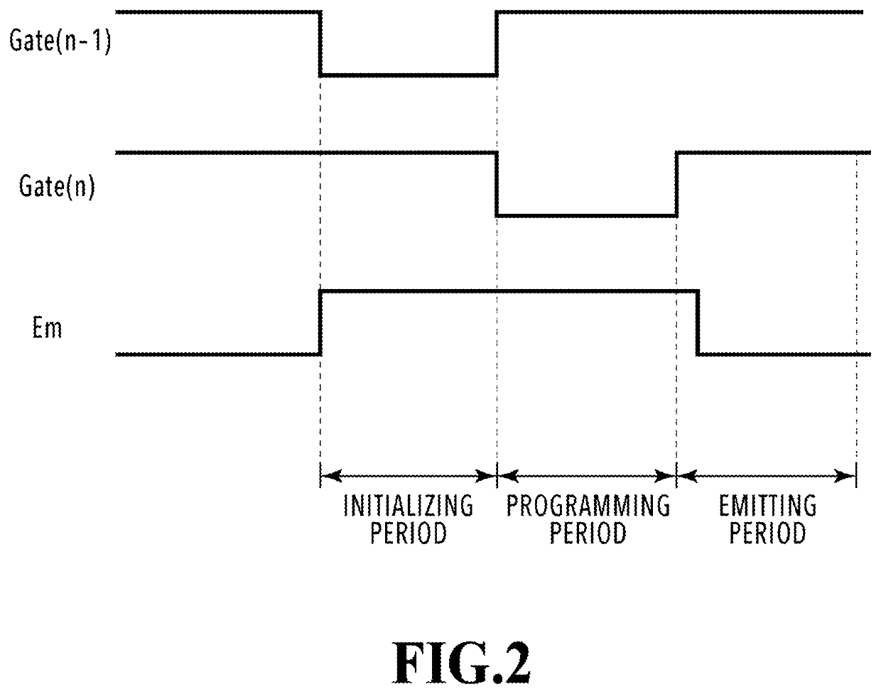
[0046]First, the operational principle of the present embodiment will be described with reference to FIGS. 1 to 4.

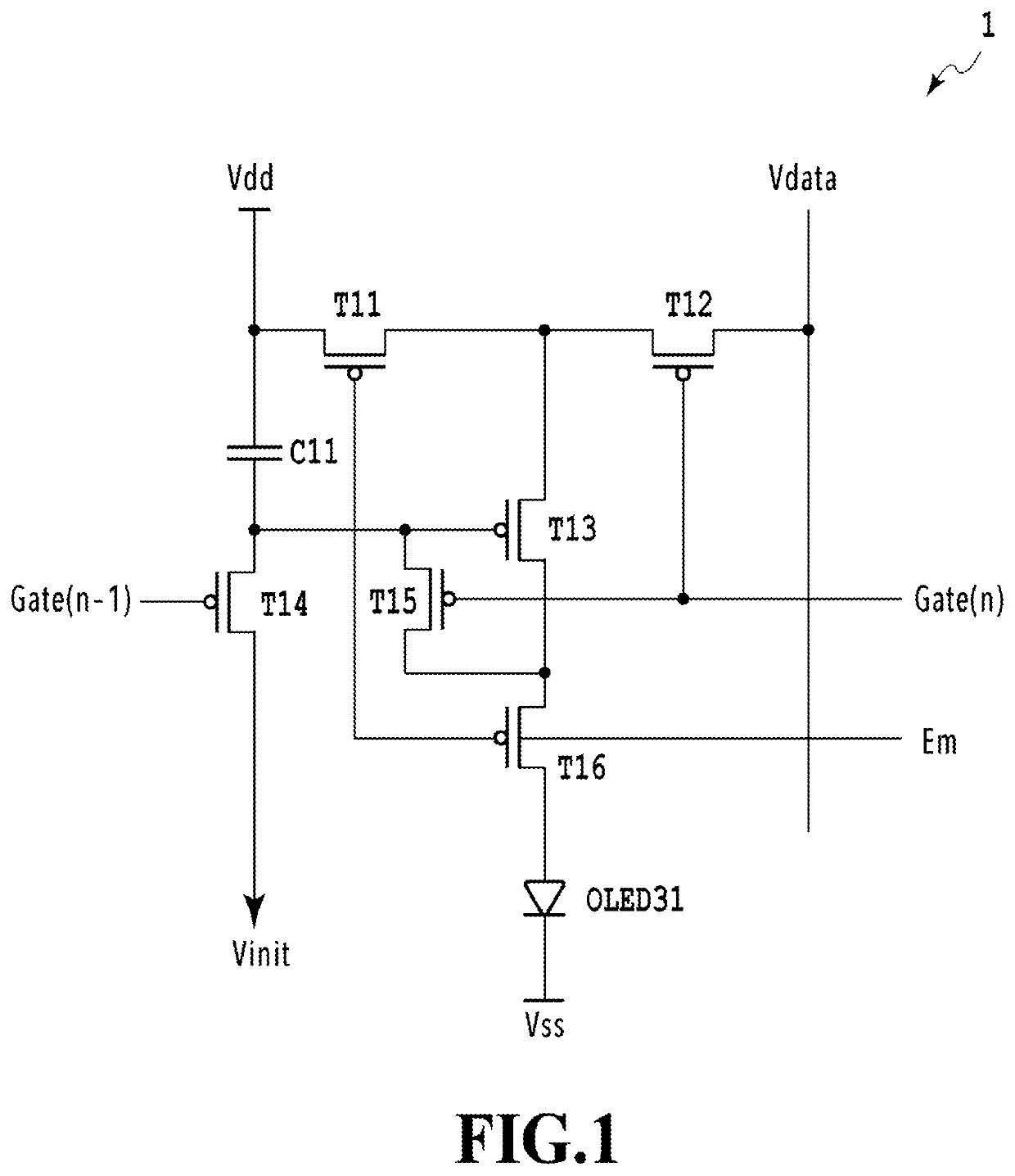
[0047]FIG. 1 is a diagram showing an example of the configuration of a 6T1C circuit which is a pixel unit drive circuit used in an OLED. This pixel unit drive circuit 1 drives and controls pixels for each pixel unit; one subpixel corresponds to a pixel unit in the following description. This pixel unit drive circuit 1 includes one OLED 31, six transistors T11 to T16, and one capacitor C11. One OLED 31 corresponds to a subpixel of one color in red (R), green (G) and blue (B) subpixels constituting one pixel.

[0048]The pixel unit drive circuit 1 includes the switching transistor T12 for, in response to a scan (gate) signal Gate(n) applied to an nth scan line, switching a data signal of a voltage level Vdata applied to the corresponding data line. The pixel unit drive circuit 1 also includes the driving transistor T13 that supplies a drive cur...


PUM


Abstract

Provided are a pixel circuit and a pixel control method capable of quickly controlling pixels with a simpler configuration of a combination of a photosensor and a pixel circuit. The pixel circuit includes: a switching transistor for switching a data signal to be applied to a data line; a driving transistor for supplying a drive current to an organic light emitting diode (OLED) according to a charge voltage corresponding to the data signal; a compensation transistor for compensating for a threshold voltage of the driving transistor; and a photosensor having a terminal to which a bias voltage is applied, wherein the switching transistor is a dual gate transistor having a first gate connected to another terminal of the photosensor, and a second gate connected to a gate of the compensation transistor.

Description

CROSS-REFERENCE TO RELATED APPLICATIONS[0001]This application is a continuation of International Application No. PCT / CN2019 / 089595, filed on May 31, 2019, the disclosure of which is hereby incorporated by reference in its entirety.TECHNICAL FIELD[0002]The present disclosure relates to a pixel circuit and a pixel control method therefor, and, more particularly, to a pixel circuit which is applied to an organic EL display and is combined with a photosensor, and a control method for a pixel circuit.BACKGROUND ART[0003]A conventionally known organic electroluminescent (EL) display is a flat panel display that uses an organic light emitting diode (OLED) as a display element and drives the OLED by current to emit light.[0004]Generally, in the pixel circuit of an organic EL display, a driving transistor causes the current to flow to the OLED, so that the characteristics of the driving transistor are important. A thin film transistor (TFT) used as a driving transistor has a problem such tha...

Claims


Application Information

Patent Timeline
IPC IPC(8): G09G3/3233
CPCG09G3/3233G09G2310/08G09G2330/021G09G2360/144G09G2300/0861G09G2310/0262G09G2310/0251G09G2360/14G09G2300/0819G09G2360/148G09G2354/00
Inventor TAKATORI, KENICHI
Owner HUAWEI TECH CO LTD
Why Eureka
Try Eureka