Semiconductor package and semiconductor device

a semiconductor and semiconductor technology, applied in the direction of semiconductor devices, semiconductor/solid-state device details, electrical apparatus, etc., can solve the problem of limited layout and achieve the effect of enhancing the degree of freedom of layout and easiness of assembly

Active Publication Date: 2022-03-17
MITSUBISHI ELECTRIC CORP
View PDF1 Cites 0 Cited by
  • Summary
  • Abstract
  • Description
  • Claims
  • Application Information

AI Technical Summary

Benefits of technology

[0004]The technology of the present disclosure has an object to enhance a degree of freedom of layout and easiness of assembly in a semiconductor package in which a plurality of semiconductor elements and a wiring element are sealed with resin to be integrated with each other.

Problems solved by technology

Further, when the wiring element is provided at the center of the semiconductor device, a connection member of a control terminal and a connection member for main current interfere with each other, and thus there is a problem in that layout is limited.

Method used


Image

  • Semiconductor package and semiconductor device
  • Semiconductor package and semiconductor device
  • Semiconductor package and semiconductor device

Examples


first embodiment

1. First Embodiment

1.1 Introduction

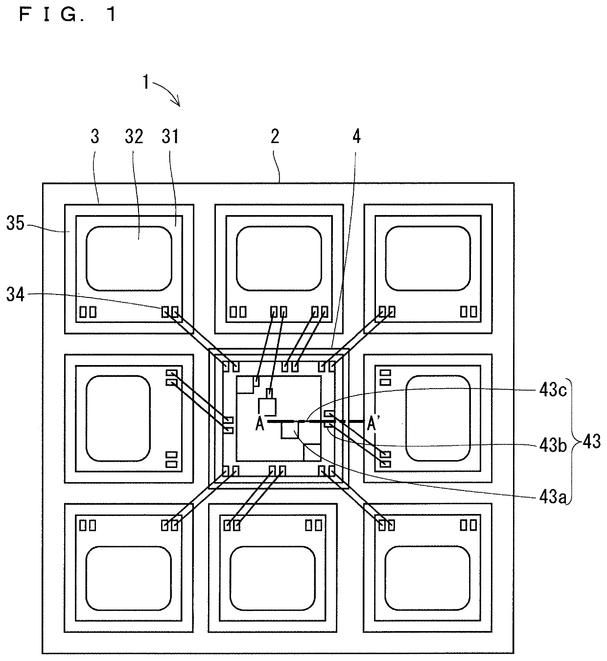
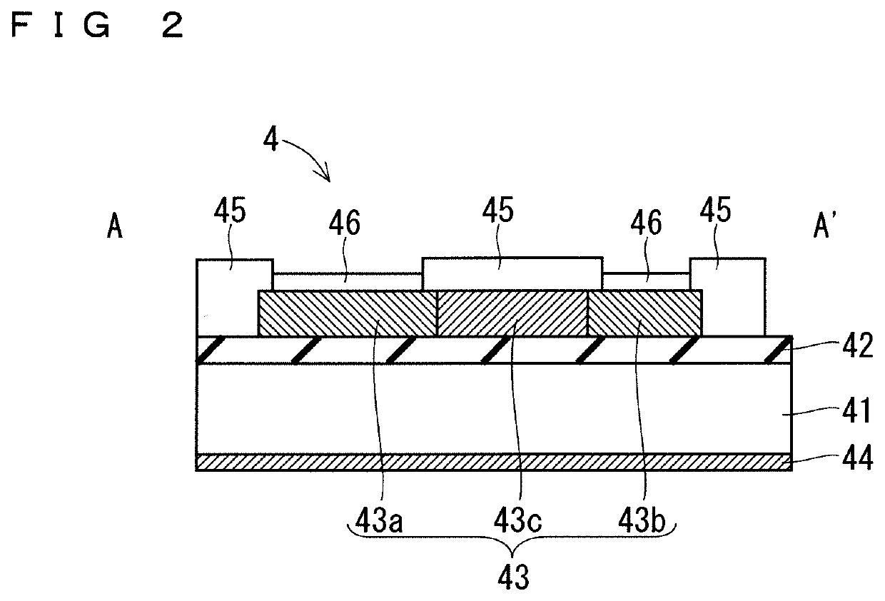
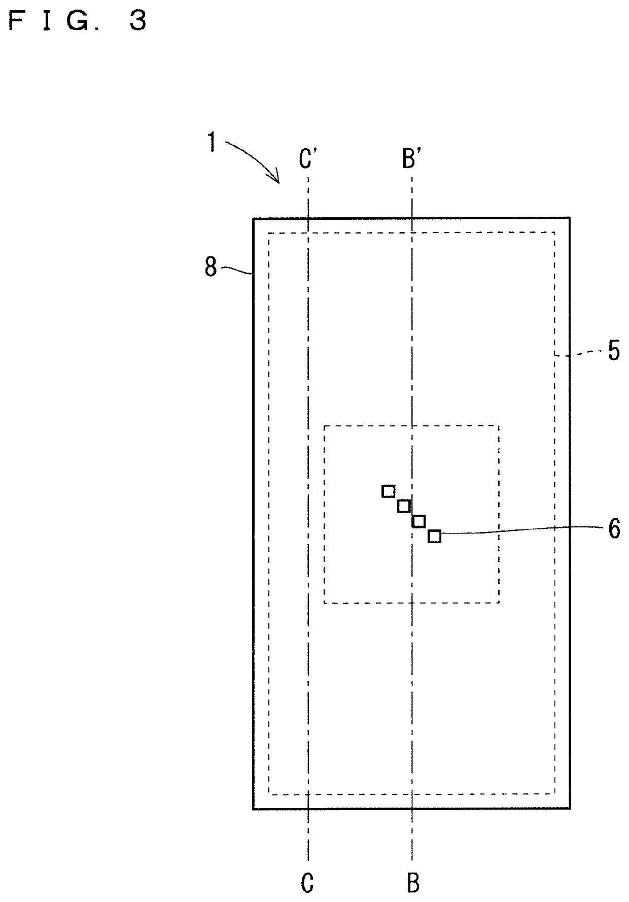
[0017]FIG. 1 is a schematic view illustrating a semiconductor package 1 according to the first embodiment. Note that a frame 5, a plurality of terminal blocks 6, a spacer conductor 7, and a sealing material 8 that are included in the semiconductor package 1 are omitted from illustration of FIG. 1 for the sake of convenience of illustration, and are illustrated in FIG. 3 to FIG. 6.

[0018]As illustrated in FIG. 1, the semiconductor package 1 includes a conductor substrate 2, a plurality of semiconductor elements 3, and a wiring element 4. It is only necessary that the number of semiconductor elements 3 be two or more. Further, it is only necessary that the number of wiring elements 4 be less than the number of semiconductor elements 3. FIG. 1 illustrates the semiconductor package 1 that includes eight semiconductor elements 3 and one wiring element 4, and the following description will describe this semiconductor package 1.

[0019]Each semiconductor ele...


PUM

PropertyMeasurementUnit
degree of freedomaaaaaaaaaa
currentaaaaaaaaaa
angleaaaaaaaaaa

Abstract

Each of a plurality of semiconductor elements included in a semiconductor package includes a front-surface electrode being provided on a semiconductor substrate on a side opposite to a conductor substrate, a back-surface electrode being joined to the conductor substrate, a control pad configured to control current flowing between the front-surface electrode and the back-surface electrode, a frame being electrically connected to the front-surface electrode, a portion of the frame being exposed from a surface of a sealing material from which a lower surface of the conductor substrate is exposed, and a plurality of terminal blocks being electrically connected to a plurality of first pads, a portion of the plurality of terminal blocks being exposed from a surface of the sealing material, the surface being provided on a side opposite to the surface of the sealing material from which the lower surface of the conductor substrate is exposed.

Description

BACKGROUND OF THE INVENTIONField of the Invention[0001]The present disclosure relates to a semiconductor package and a semiconductor device.Description of the Background Art[0002]WO 2010 / 110170 A1 discloses a semiconductor device having a configuration in which a plurality of semiconductor elements and a wiring element are sealed with resin to be integrated with each other.[0003]In the semiconductor device described in WO 2010 / 110170 A1, for example, an external connection member, such as wire bonding or a lead frame, is required to be provided in order to connect a source electrode to an external circuit. Further, when the wiring element is provided at the center of the semiconductor device, a connection member of a control terminal and a connection member for main current interfere with each other, and thus there is a problem in that layout is limited.SUMMARY[0004]The technology of the present disclosure has an object to enhance a degree of freedom of layout and easiness of assemb...

Claims


Application Information

Patent Timeline
Patent Type & Authority Applications(United States)
IPC IPC(8): H01L25/07H01L23/492H01L23/538H01L23/31H01L23/498H01L23/16
CPCH01L25/072H01L23/492H01L23/16H01L23/3121H01L23/49844H01L23/5386H01L23/488H01L23/49H01L23/4952H01L23/49575H01L24/47H01L23/315H01L2224/0603H01L2224/45144H01L2224/45139H01L2224/45124H01L24/05H01L23/147H01L23/49811H01L24/45H01L2224/8384H01L2224/29339H01L2224/29347H01L2924/181H01L2924/1815H01L2224/06181H01L2924/13091H01L2924/13055H01L2224/49175H01L24/06H01L2224/33181H01L24/29H01L24/33H01L24/49H01L2224/49171H01L2224/05554H01L2224/04042H01L2224/0612H01L24/48H01L24/32H01L2224/73265H01L2224/04026H01L2224/48157H01L24/73H01L24/83H01L2224/32245H01L2224/05647H01L2224/05124H01L2224/85447H01L2224/05644H01L2224/85444H01L2224/05655H01L2224/05639H01L2224/85455H01L2224/85439H01L2224/83399H01L2924/00014H01L2924/00012H01L2924/00
Inventor NAKATA, YOSUKE
Owner MITSUBISHI ELECTRIC CORP
Why Eureka
Try Eureka