Wafer manufacturing method

Pending Publication Date: 2022-03-24
DISCO CORP
View PDF4 Cites 0 Cited by
  • Summary
  • Abstract
  • Description
  • Claims
  • Application Information

AI Technical Summary

Benefits of technology

[0011]According to the wafer manufacturing method of the present invention, the separation layer can be formed at t

Problems solved by technology

Although the technique disclosed in Japanese Patent Laid-open No. 2016-111143 enables efficient

Method used


Image

  • Wafer manufacturing method
  • Wafer manufacturing method
  • Wafer manufacturing method

Examples


Example

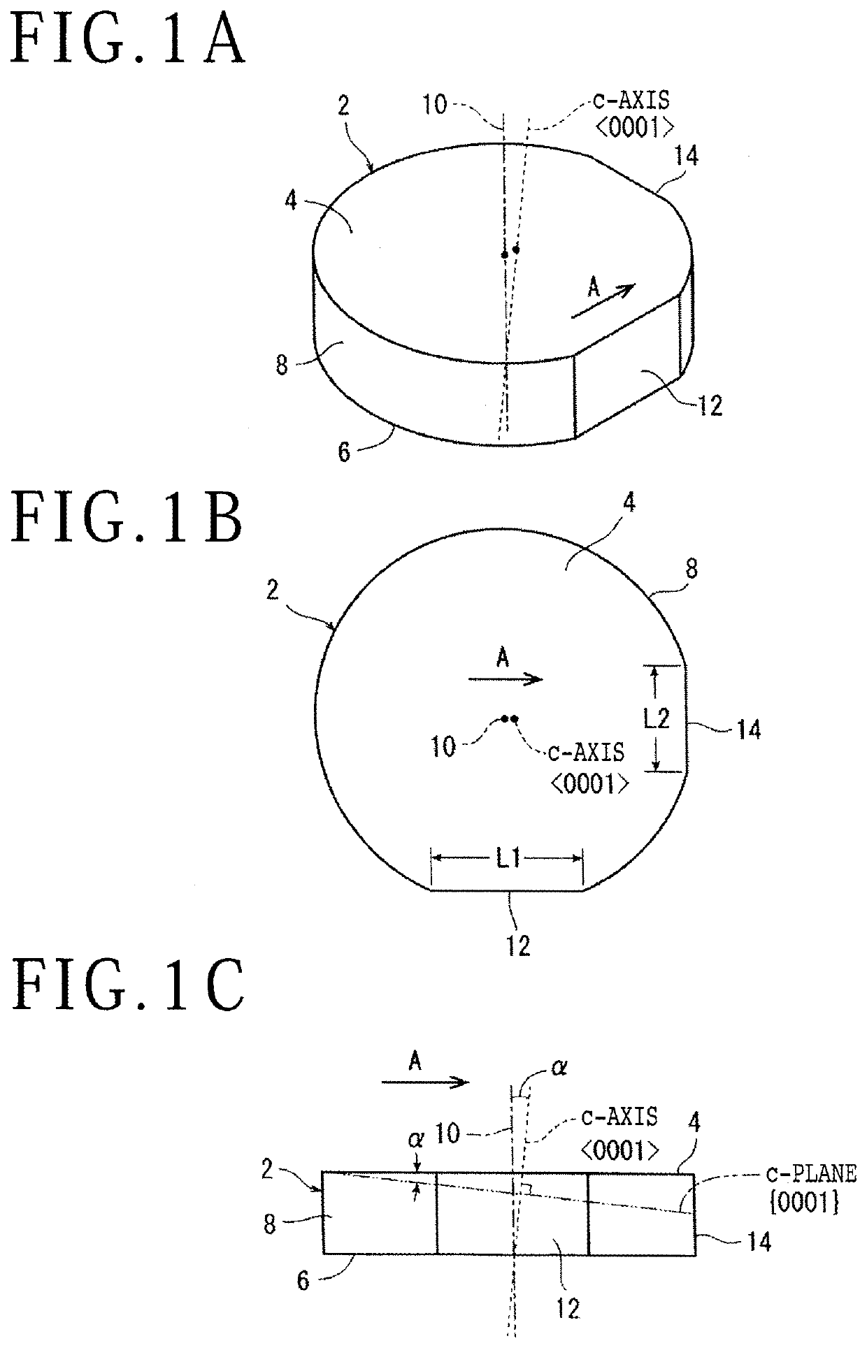
[0032]A preferred embodiment of the present invention will be described below with reference to the drawings. In FIGS. 1A to 1C, a circular columnar silicon carbide (SiC) ingot 2 that can be used for the wafer manufacturing method of the present invention is illustrated. The SiC ingot 2 is formed from hexagonal single-crystal SiC. The SiC ingot 2 has a circular first end surface 4, a circular second end surface 6 on a side opposite to the first end surface 4, a circumferential surface 8 located between the first end surface 4 and the second end surface 6, a c-axis (0001> direction) that reaches the second end surface 6 from the first end surface 4, and a c-plane ({0001} plane) orthogonal to the c-axis. At least the first end surface 4 is planarized by grinding or polishing to such an extent that incidence of a laser beam is not precluded.

[0033]In the SiC ingot 2, the c-axis is inclined with respect to a perpendicular line 10 to the first end surface 4, and an off-angle α (for exampl...


PUM

PropertyMeasurementUnit
Angleaaaaaaaaaa

Abstract

A wafer manufacturing method includes a Z-coordinate measurement step of deeming a separation layer to be formed as an XY plane and measuring a height Z(X, Y) of an upper surface of an ingot to be irradiated with a laser beam, corresponding to the X-coordinate and the Y-coordinate, and a calculation step of defining a Z-coordinate of the separation layer to be formed as Z0 and calculating a difference from the measured height Z(X, Y) (Z(X, Y)-Z0) to obtain a Z-coordinate of a beam condenser. A separation layer is formed by relatively moving the beam condenser in an X-axis direction and a Y-axis direction. The beam condenser is moved in a Z-axis direction on the basis of the Z-coordinate obtained in the calculation step to position a focal point to Z0, and the separation layer is formed. A wafer is separated from the ingot.

Description

BACKGROUND OF THE INVENTIONField of the Invention[0001]The present invention relates to a wafer manufacturing method in which a focal point of a laser beam with a wavelength having transmissibility with respect to a semiconductor ingot (hereinafter, abbreviated simply as an ingot) is positioned inside the ingot from an end surface of the ingot, the ingot is irradiated with the laser beam to form a separation layer, and a wafer is manufactured from the separation layer.Description of the Related Art[0002]A wafer on which plural devices such as integrated circuits (ICs) and large scale integration (LSI) circuits are formed on a front surface in such a manner as to be marked out by plural planned dividing lines that intersect is divided into individual device chips by a dicing apparatus or a laser processing apparatus. The respective device chips obtained by the dividing are used for pieces of electrical equipment such as portable phones and personal computers.[0003]A silicon (Si) subs...

Claims


Application Information

Patent Timeline
IPC IPC(8): B23K26/364
CPCB23K26/364B28D5/04B28D5/0082B28D5/0058H01L21/78B23K26/53B23K2103/56B23K26/048B23K26/38B23K26/0876B23K26/0648H01L21/0445B23K2101/40
Inventor HIRATA, KAZUYA
Owner DISCO CORP
Why Eureka
Try Eureka