

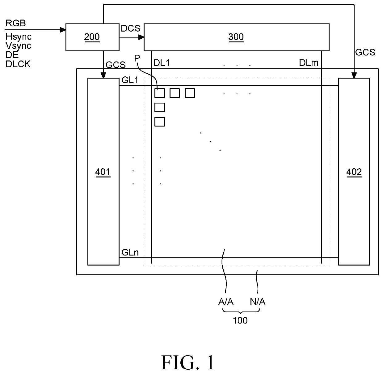
Pixel and Organic Light Emitting Display Device Comprising the Same
a technology of light-emitting display device and pixel, which is applied in the direction of semiconductor devices, instruments, electrical apparatus, etc., can solve the problems of uneven luminance of pixels and unstable driving current of high-potential voltage, and achieve the effect of reducing the instability of driving curren
- Summary
- Abstract
- Description
- Claims
- Application Information
AI Technical Summary
Benefits of technology
Problems solved by technology
Method used
Image

Examples
second exemplary embodiment
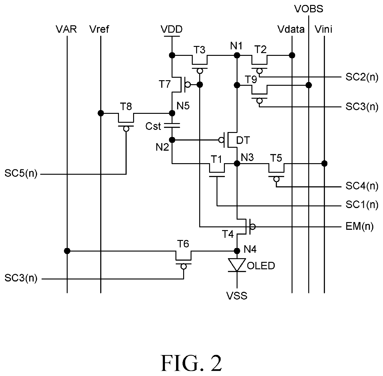
[0129]FIG. 7 is a circuit diagram of a pixel of an organic light emitting display device according to another exemplary embodiment of the present disclosure.
[0130]In the organic light emitting display device according to another exemplary embodiment of the present disclosure, each pixel P includes an organic light emitting diode OLED, a driving transistor DT, first to eighth transistors T1 to T8, and a capacitor Cst.
[0131]The driving transistor DT controls a driving current applied to the organic light emitting diode OLED according to a source-gate voltage Vsg thereof. The driving transistor DT may be a p-type MOSFET PMOS and may be a low-temperature polycrystalline silicon (LTPS) thin film transistor. In addition, a source electrode of the driving transistor DT is connected to a first node N1, a gate electrode thereof is connected to a second node N2, and a drain electrode thereof is connected to a third node N3.
[0132]The first transistor T1 connects the gate electrode and the drai...
third exemplary embodiment
[0165]FIG. 11 is a circuit diagram illustrating a pixel of an organic light emitting display device according to yet another (third) exemplary embodiment of the present disclosure.
[0166]In the organic light emitting display device according to yet another (third) exemplary embodiment of the present disclosure, each pixel P includes an organic light emitting diode OLED, a driving transistor DT, first to eighth transistors T1 to T8, and a capacitor Cst.
[0167]The driving transistor DT controls a driving current applied to the organic light emitting diode OLED according to a source-gate voltage Vsg thereof. The driving transistor DT may be a p-type MOSFET PMOS and may be a low temperature polycrystalline silicon (LTPS) thin film transistor. In addition, a source electrode of the driving transistor DT is connected to a first node N1, a gate electrode thereof is connected to a second node N2, and a drain electrode thereof is connected to a third node N3.
[0168]The first transistor T1 conne...
fourth exemplary embodiment
[0204]FIG. 15 is a circuit diagram illustrating a pixel of the organic light emitting display device according to yet another (fourth) exemplary embodiment of the present disclosure.
[0205]In the organic light emitting display device according to yet another (fourth) exemplary embodiment of the present disclosure, each pixel P includes an organic light emitting diode OLED, a driving transistor DT, first to eighth transistors T1 to T8, and a capacitor Cst.
[0206]The driving transistor DT controls a driving current applied to the organic light emitting diode OLED according to a source-gate voltage Vsg thereof. The driving transistor DT may be a p-type MOSFET PMOS and may be a low temperature polycrystalline silicon (LTPS) thin film transistor. In addition, a source electrode of the driving transistor DT is connected to a first node N1, a gate electrode thereof is connected to a second node N2, and a drain electrode thereof is connected to a third node N3.
[0207]The first transistor T1 co...
PUM
 Abstract
Description
Claims
Application Information