Packaging substrate, and semiconductor device comprising same
a technology of packaging substrate and semiconductor device, which is applied in the direction of semiconductor device details, semiconductor/solid-state device devices, electrical apparatus, etc., can solve the problems of difficult mounting of high-performance and high-frequency semiconductor elements thereon, distinct limitation to the reduction of wiring pitch, and inability to fully support packaging technology. , to achieve the effect of improving electrical properties, simplifying the treatment process of an insulating layer, and relatively easy mass production
- Summary
- Abstract
- Description
- Claims
- Application Information
AI Technical Summary
Benefits of technology
Problems solved by technology
Method used
Image

Examples
example 1
ring of a Packaging Substrate
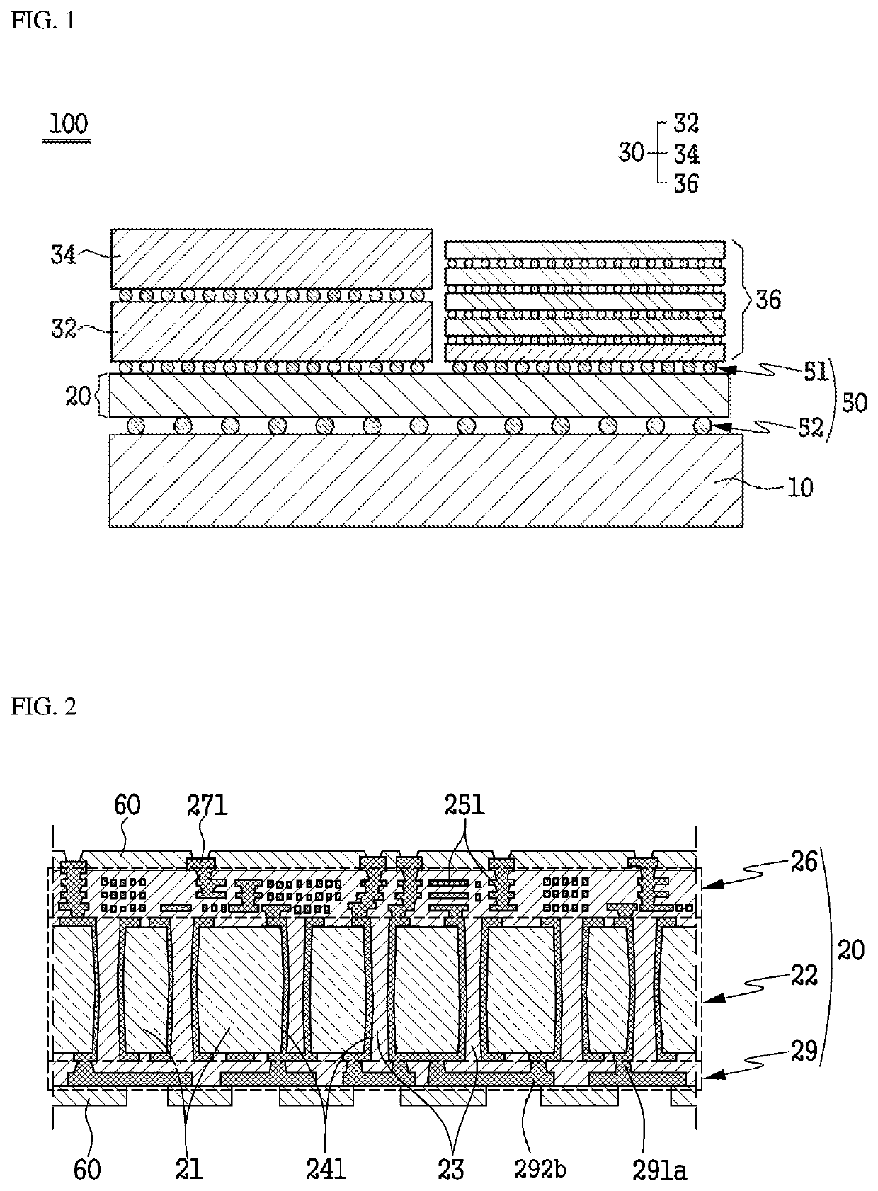
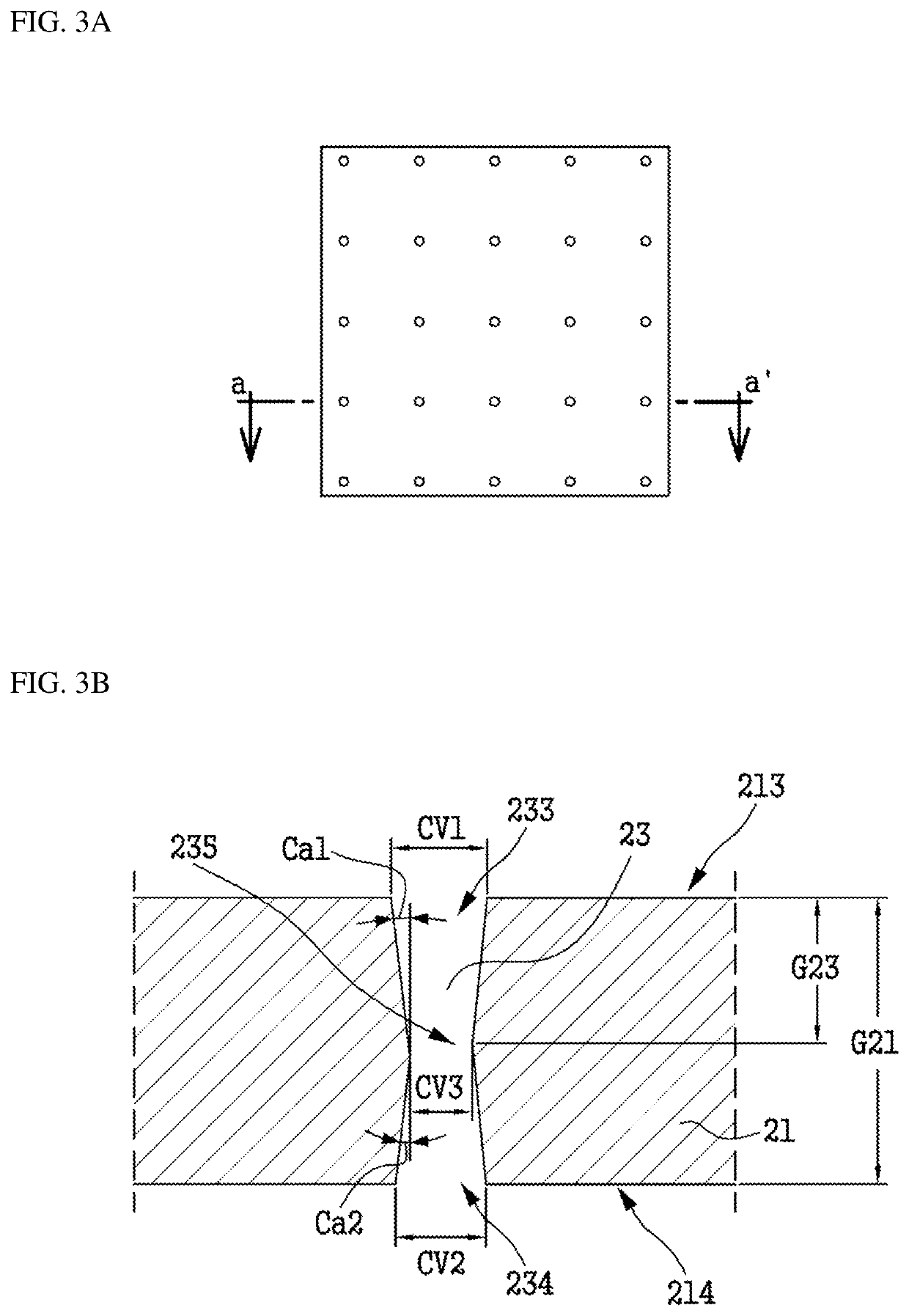
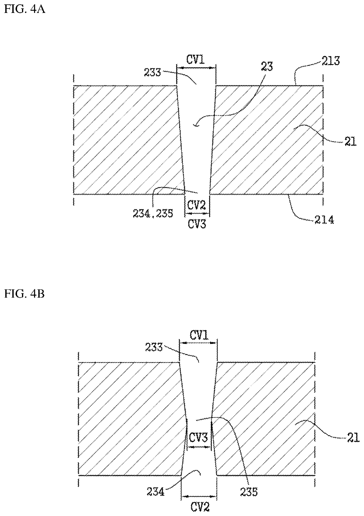
[0151]1) Preparation Step (Glass Defect Forming Process): A glass substrate 21a with a flat first surface and a flat second surface was prepared, and defects (grooves, 21b) were formed on the glass surface at a predetermined position for forming a core via. In this case, the number of defects were allowed to form in the number of 225 per 1 cm2. As the glass, borosilicate glass (from CORNING) was applied. A method of mechanical etching and laser irradiation were applied to the formation of the defect (groove).
[0152]2) Etching Step (Core Via Forming Step): The core via 23 was formed on the glass substrate 21a where the defects (grooves, 21b) were formed, through a physical or chemical etching process. The etching was performed by a method of placing the glass substrate in an etching bath filled with 2 M hydrofluoric acid (HF), 1.1 M nitric acid (HNO3) and deionized water, and applying ultrasonic waves at 80 Hz and 100% output.
[0153]Also, the core via were ...
example 2
ring of a Packaging Substrate
[0160]A packaging substrate was manufactured in the same manner as in Example 1, except for changing the conditions in the Example 1 to 1.1 M hydrofluoric acid, and 80% ultrasonic output during etching.
example 3
ring of a Packaging Substrate
[0161]A packaging substrate was manufactured in the same manner as in Example 1, except for changing the conditions in the Example 1 to 60% ultrasonic output during etching.
PUM
| Property | Measurement | Unit |
|---|---|---|
| inner diameter | aaaaa | aaaaa |
| diameter | aaaaa | aaaaa |
| diameter | aaaaa | aaaaa |
Abstract
Description
Claims
Application Information
 - R&D Engineer
- R&D Manager
- IP Professional
- Industry Leading Data Capabilities
- Powerful AI technology
- Patent DNA Extraction
Browse by: Latest US Patents, China's latest patents, Technical Efficacy Thesaurus, Application Domain, Technology Topic.
© 2024 PatSnap. All rights reserved.Legal|Privacy policy|Modern Slavery Act Transparency Statement|Sitemap