
Beam imaging and profiling device

a beam imaging and profiling technology, applied in the direction of radiation controlled devices, optical radiation measurement, instruments, etc., can solve the problems of inaccurate readings, damage and change in responsivity, and serious limitations of existing imaging systems, and achieve accurate and reliable production of images or beam profile information. high accuracy

Inactive Publication Date: 2022-06-02
STAR TECH INSTR
View PDF7 Cites 0 Cited by
  • Summary
  • Abstract
  • Description
  • Claims
  • Application Information

AI Technical Summary

Benefits of technology

The present invention is about a sensor that is not negatively impacted by UV / X-ray radiation and can produce accurate and reliable results without requiring frequent recalibrations or replacements. The sensor downconverts the UV / X-ray beam to visible light and uses an image sensor to capture the information about the beam. This setup protects the sensor from the direct impact of the UV / X-ray beam and ensures long-term accuracy.

Problems solved by technology

Existing imaging systems have serious limitations.
Degradation of the imaging and the optical elements due to exposure by the beam can result in damage and change in responsivity.
This results in inaccurate readings over time and requires re-calibration or replacement of the sensor and / or the optical members.

Method used


Image

  • Beam imaging and profiling device
  • Beam imaging and profiling device

Examples


Embodiment Construction

[0025]The present invention now will be described more fully hereinafter with reference to the accompanying figures, in which exemplary embodiments of the invention are shown. The invention may, however, be embodied in many different forms and should not be construed as limited to the embodiments set forth herein. Like reference numerals refer to like elements throughout.

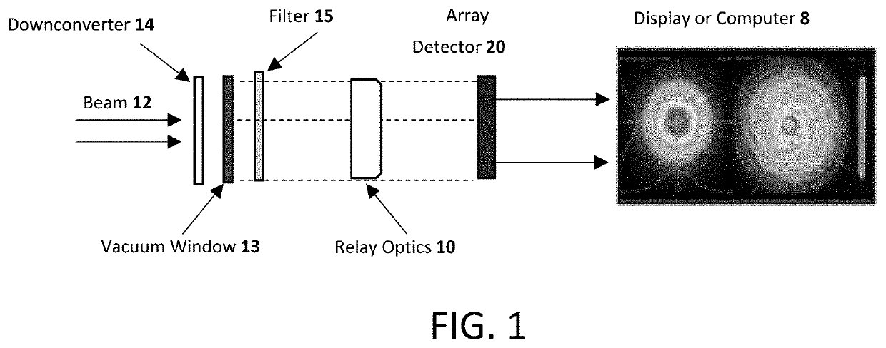
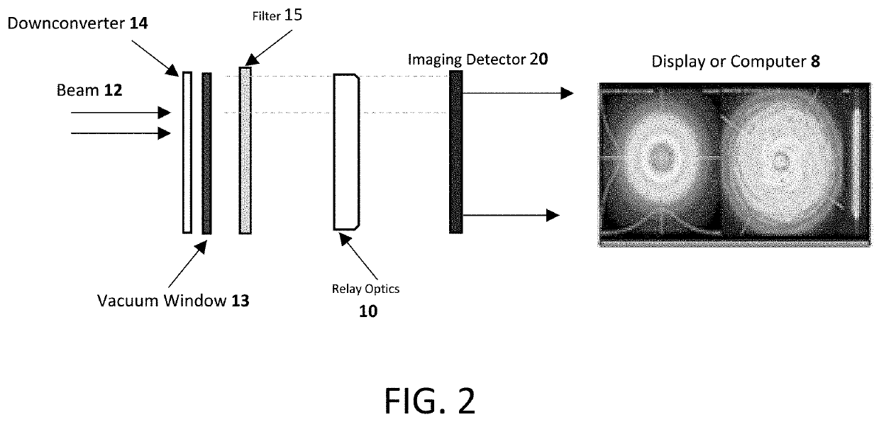
[0026]Referring now to FIGS. 1 and 2, therein illustrated are schematics of exemplary image sensors according to an aspect of the present invention. The image sensors are generally configured to receive a beam 12, which may be a VUV, XUV, X-ray, Soft X-ray or the like beam having about a 1 to 200 nm wavelength, down-convert the beam 12 into longer wavelength radiation, for example, visible, near-infrared or infrared light, relay the down-converted beam to an imaging detector 20 (or array detector) and convey the information from the imaging detector 20 to a display device 8, such as a computer. In this manner, the i...


PUM

PropertyMeasurementUnit
wavelengthaaaaaaaaaa

Abstract

Exemplary aspects of the present invention are directed to an imaging sensor system for beams in the 1-200 nm spectral regions. The system may include a downconverter for converting the beam to visible light, optical filter elements, and relay optics for directing the visible light to the imaging detector. The relay optics convey the image and / or optical beam profile intensity to a 2-D imaging array such as CMOS, CCD (or other imaging detector device). The system can be used in a vacuum or in ambient non-vacuum conditions which may include a purged environment.

Description

CROSS-REFERENCE TO RELATED APPLICATIONS[0001]This application claims priority to U.S. Provisional Appl. No. 63 / 120,393 filed Dec. 2, 2020, which is hereby incorporated by reference in its entirety.BACKGROUND OF THE INVENTION1. Field of the Invention[0002]The present invention is directed to a beam imaging and profiling device, and more particularly to an imaging sensor for the 1 to 200 nm spectral regions.2. Related Art[0003]New technological advances require new solutions for high resolution imaging in the VUV, XUV, X-ray and soft X-ray regions (1-200 nm). These developments have necessitated unique solutions for analyzers and diagnostic tools. The applications include, but are not limited to: microlithography, microbiology, medical and diagnostic metrology. These new applications require increased resolution and push the development of new measurement capabilities or the deep UV and X-ray regions. Existing imaging systems have serious limitations. Degradation of the imaging and th...

Claims


Application Information

Patent Timeline
Patent Type & Authority Applications(United States)
IPC IPC(8): H01L27/146G01J1/58G02B13/14
CPCH01L27/14625G02B13/143G01J1/58H01L27/14676G01J1/4257G02B5/208G01J1/0488G01J1/429G01J2001/448
Inventor FRICKE, WILLIAM C.GANOPOULOS, MIKEMARTIN, CLIFFORD A.WILSON, JOHN K.
Owner STAR TECH INSTR
Learn More