Circuit for Switching Power Supply and Switching Power Supply Device

a technology of switching power supply and circuit, applied in the direction of pulse technique, process and machine control, instruments, etc., can solve the problems of increasing heat generation and increasing heat generation

Active Publication Date: 2022-06-30
ROHM CO LTD
View PDF1 Cites 0 Cited by
  • Summary
  • Abstract
  • Description
  • Claims
  • Application Information

AI Technical Summary

Problems solved by technology

At this point, there is a concern that accumulated charge of the output capacitor may form a discharging parasitic diode at the high-side transistor that is configured as a metal-oxide-semiconductor field-effect transistor (MOSFET), and this generates more heat.
Moreover, when the high-side transistor and...

Method used


Image

  • Circuit for Switching Power Supply and Switching Power Supply Device
  • Circuit for Switching Power Supply and Switching Power Supply Device
  • Circuit for Switching Power Supply and Switching Power Supply Device

Examples


implementation example ex _ 1a

Implementation Example EX_1A

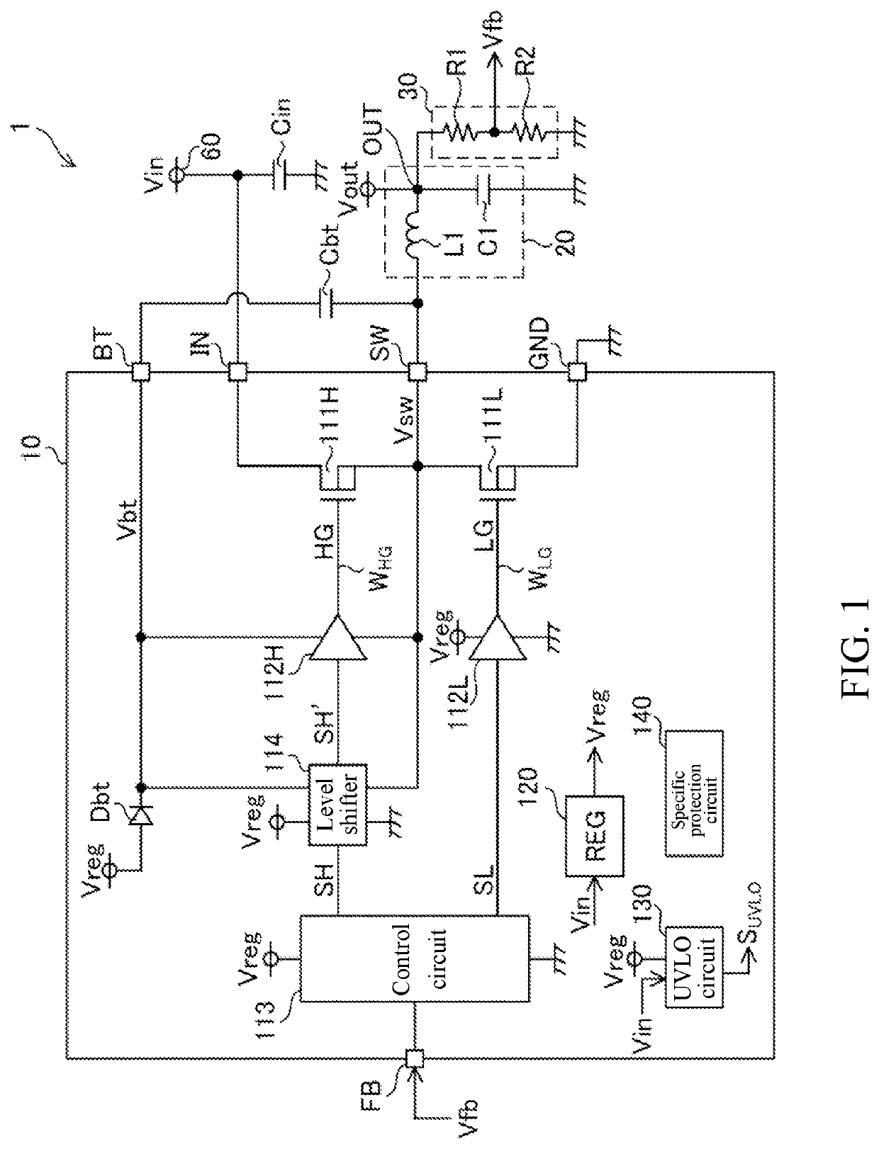
[0067]Implementation example EX_1A is described below. In implementation example EX_1A, the configuration and operation beneficial to the first case are described. The specific protection circuit 140 in implementation example EX_1 A includes a comparator CMP shown in FIG. 9. The comparator CMP compares the input voltage Vin at the input terminal IN with the switch voltage Vsw of the switch terminal SW, and outputs a signal CMPout corresponding to the comparison result. The comparison signal CMPout is a binary signal adopting a high level or a low level. A positive-side power voltage of the comparator CMP is the internal power voltage Vreg, and a negative-side power voltage of the comparator CMP is the ground. Thus, the high level of the signal CMPout is substantially the same as the level of the internal power voltage Vreg, and the low level of the signal CMPout is substantially the same as the level of the ground.

[0068]The input voltage Vin is input to t...

implementation example ex _ 1b

Implementation Example EX_1B

[0075]Implementation example EX_1B is described below. In implementation example EX_1B, the configuration and operation beneficial to the first case are also described. FIG. 10 shows a main part of the configuration related to the implementation example EX_1B. The specific protection circuit 140 in implementation example EX_1B includes a protection transistor 221, a resistor 222 and a switch 223. The protection transistor 221 is a P-channel MOSFET.

[0076]In the protection transistor 221, the switch voltage Vsw is applied to the source, and the input voltage Vin is applied to the gate. The drain of the protection transistor 221 is connected to one end portion of the resistor 222 via a node 224, and the other end portion of the resistor 222 is grounded. The node 224 is connected to a control terminal of the switch 223. One terminal of the switch 223 is connected to the boot terminal BT and a wire Wbt connected to the cathode of the diode Dbt. Thus, the boot ...

implementation example ex _ 1c

Implementation Example EX_1C

[0082]Implementation example EX_1C is described below. In implementation example EX_1C, the configuration and operation beneficial to the first case are also described. FIG. 11 shows a main part of the configuration related to the implementation example EX_1C. The specific protection circuit 140 in implementation example EX_1C includes a protection transistor 231 and a resistor 232. The protection transistor 231 is a P-channel MOSFET.

[0083]In the protection transistor 231, the switch voltage Vsw is applied to the source, and the input voltage Vin is applied to the gate. The drain of the protection transistor 231 is connected to one end portion of the resistor 232 via a node 234, and the other end portion of the resistor 232 is grounded. The node 234 is connected to a wire WLG.

[0084]A voltage as a voltage drop of the resistor 232 is generated at the node 234. When the switch voltage Vsw is caused to be above the input voltage Vin due damage such as short-c...


PUM


Abstract

The present disclosure provides a power integrated circuit (IC) for a switching power supply device that generates an output voltage based on an input voltage. The circuit includes: a high-side transistor, disposed between an input terminal applied with the input voltage and a switch terminal; and a low-side transistor, disposed between the switch terminal and a ground terminal. A feedback control for turning on or off the transistor is performed based on a feedback voltage corresponding to the output voltage. A protection circuit is capable of performing a protection operation for turning on the high-side transistor or the low-side transistor regardless of the feedback control based on a switch voltage at the switch terminal and the input voltage, based on a backflow current from the ground terminal to the switch terminal, or based on the input voltage and a predetermined determination voltage.

Description

TECHNICAL FIELD[0001]The present disclosure relates to a circuit for switching power supply and a switching power supply device.BACKGROUND[0002]A certain type of switching power supply device has a series circuit having a high-side transistor and a low-side transistor, and a direct-current (DC) input voltage is applied to the series circuit. The input voltage is maintained by an input capacitor. Moreover, a voltage having a rectangular waveform obtained by alternately turning on and turning off the high-side transistor and the low-side transistor is rectified and smoothed using a coil and an output capacitor. Accordingly, a DC output voltage stepped down from the input voltage can be obtained.PRIOR ART DOCUMENTPatent Publication[0003][Patent document 1] Japan Patent Publication No. 2020-078203SUMMARYProblems to be Solved by the Disclosure[0004]In the switching power supply device above, the input voltage drastically drops to 0 V in case of damage such as short-circuitry of the input...

Claims


Application Information

Patent Timeline
IPC IPC(8): H03K17/082H02M3/156H03K17/06H03K17/687
CPCH03K17/0822H03K17/687H03K17/06H02M3/156H02M1/088H02H7/1213H02M3/158H02M1/32H02M1/08
Inventor GUAN, SHIDONG
Owner ROHM CO LTD
Why Eureka
Try Eureka