Method for forming a trench in a first semiconductor layer of a multi-layer system

Pending Publication Date: 2022-07-21
ROBERT BOSCH GMBH
View PDF0 Cites 0 Cited by
  • Summary
  • Abstract
  • Description
  • Claims
  • Application Information

AI Technical Summary

Problems solved by technology

As a result of this lesser removal, a slight overhang (“blade”) remains after removal of the mask at the upper edge of the trench, which may be subject to mechanical striking and may break off after the release of the movable structures, so that broken-off semiconductor particles or hooking of the freely movable structure may arise.
If the removal of the second semiconductor layer (situated above the hard mask) and the trench formation in the first semiconductor layer (situated beneath the mask layer) are carried out in a continu

Method used


Image

  • Method for forming a trench in a first semiconductor layer of a multi-layer system
  • Method for forming a trench in a first semiconductor layer of a multi-layer system
  • Method for forming a trench in a first semiconductor layer of a multi-layer system

Examples


Embodiment Construction

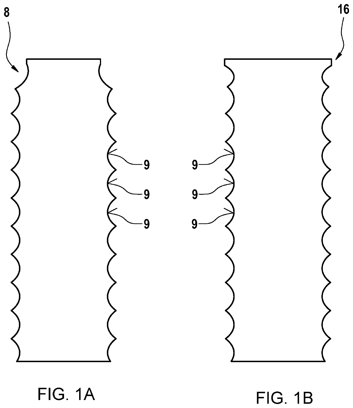
[0025]FIGS. 1A and 1B schematically illustrates two structures generated by trench etching using deep reactive ion etching (DRIE). The two structures may, for example, be deflectable masses of a microelectromechanical system. The vertically extending walls are formed by a cyclical alternation between etching and passivation steps, so that grooves 9 typical of this method arise at the trench wall. In the process, the width (i.e., the horizontal extension with respect to the drawing plane) of the trenches and of the generated structures is defined by an etching mask, which is removed after the trenches have been formed. As is shown to the right in FIG. 1B, a slightly lesser material removal takes place directly beneath the etching mask at the upper edge of the trench, so that an overhang 16 (“blade”) remains there after the removal of the etching mask. This “blade”16 may impinge on an adjoining structure and break off during a deflection of the movable mass or result in hooking. To av...


PUM


Abstract

A method for forming a trench in a first semiconductor layer of a multi-layer system. The method includes: applying a mask layer onto the first semiconductor layer, a recess being formed in the mask layer so that the first semiconductor layer is exposed within the recess; applying a protective layer which completely covers or modifies the first semiconductor layer exposed within the recess; applying a second semiconductor layer; etching the second semiconductor layer to completely remove it in a subarea surrounding the recess of the mask layer; etching the protective layer so that the first semiconductor layer is exposed within the recess; and forming the trench in the first semiconductor layer, the recess of the mask layer serving as an etching mask, and the trench being formed by a cyclical alternation between etching and passivation steps, the first etching step being longer than the subsequent etching steps.

Description

FIELD[0001]The present invention is directed to a method for forming a trench in a first semiconductor layer of a multi-layer system.BACKGROUND INFORMATION[0002]Conventional methods for structuring semiconductor layers with the aid of trench etching (trenching) from the related art are available in numerous specific embodiments. For example, structures which, provided with corresponding electrical contacting, may act as movable masses are exposed by one or multiple trench(es) during the manufacture of microelectromechanical systems (MEMS). For this purpose, the MEMS functional trench using deep reactive ion etching (DRIE) is described, in particular, in U.S. Pat. No. 5,501,893 A (“Method of anisotropically etching silicon”), in which a trench including almost perfectly vertically extending inner walls may be formed in a semiconductor layer via a cyclical sequence of etching and passivation steps. In the process, however, the material removal progresses slightly more slowly directly ...

Claims


Application Information

Patent Timeline
IPC IPC(8): H01L21/308H01L21/3065H01L21/311H01L21/66
CPCH01L21/308H01L22/26H01L21/31116H01L21/3065H01L21/3086B81C1/00523B81C1/00531B81C1/00388H01L21/3083H01L21/30655B81C2201/0112B81B2203/033B81C1/00428B81C2201/0198
Inventor SCHWENK, CHRISTOFSCHORR, NICOLAS
Owner ROBERT BOSCH GMBH
Why Eureka
Try Eureka