
Semiconductor test apparatus and semiconductor test method

a test apparatus and semiconductor technology, applied in the direction of individual semiconductor device testing, semiconductor/solid-state device testing/measurement, instruments, etc., can solve the problems of pressure loss increasing proportional to the length of the vacuum passage, and the measurement accuracy of the semiconductor test is reduced, so as to suppress the lowering of measurement accuracy

Pending Publication Date: 2022-08-04
MITSUBISHI ELECTRIC CORP
View PDF4 Cites 0 Cited by
  • Summary
  • Abstract
  • Description
  • Claims
  • Application Information

AI Technical Summary

Benefits of technology

The present invention provides a technique to prevent errors in measuring semiconductor wafers during testing. This is achieved by reducing the variation in the contact resistance between the wafer and the chuck, which results in a smaller variation in suction force. This technique ensures accurate measurements and prevents errors caused by variations in contact resistance.

Problems solved by technology

However, in the technique described in Japanese Patent Application Laid-Open No. 2015-26765, a semiconductor wafer is sucked through the vacuum passage; therefore, the pressure loss increases in proportion to the length of the vacuum passage.
There has been a problem that the measurement accuracy of the semiconductor test lowers as a result of the variation in contact resistance between the semiconductor wafer and the chuck top.

Method used


Image

  • Semiconductor test apparatus and semiconductor test method
  • Semiconductor test apparatus and semiconductor test method
  • Semiconductor test apparatus and semiconductor test method

Examples


embodiment 1

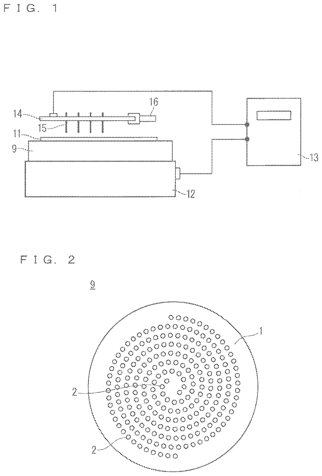
[0026]Hereinafter, Embodiment 1 will be described with reference to the drawings. FIG. 1 is a schematic view of a semiconductor test apparatus according to Embodiment 1.

[0027]As illustrated in FIG. 1, the semiconductor test apparatus includes a chuck stage 12, a chuck top 9, a tester 13, a test jig 14, contact probes 15, and a transfer arm 16. The semiconductor test apparatus further includes a control unit (not illustrated) that controls each part of the semiconductor test apparatus, a transport hand (not illustrated) for mounting a semiconductor wafer 11 on the chuck top 9, a sensor (not illustrated) for capturing features of the semiconductor wafer 11. Here, the control unit is, for example, a processor.

[0028]The chuck top 9 is mounted on the upper surface of the chuck stage 12. The semiconductor wafer 11 subject to the semiconductor test is placed on the upper surface of the chuck top 9.

[0029]The test jig 14 is held by the transfer arm 16 so as to be located above the semiconduc...

embodiment 2

[0051]Next, a semiconductor test apparatus according to Embodiment 2 will be described. FIG. 6 is a top view of a chuck top 9A included in a semiconductor test apparatus according to Embodiment 2. FIG. 7 is a top view of the chuck top 9A as viewed from above the mounting table 4. FIG. 8 is a cross-sectional view taken along the line B-B of FIG. 7. In Embodiment 2, the same components as those described in Embodiment 1 are designated by the same reference numerals, and the description thereof is omitted.

[0052]In Embodiment 1, the vacuum tube 6 connected to the outer circumference portion of the flow pass 7 is provided, however, as illustrated in FIGS. 6 to 8, in Embodiment 2, the chuck top 9A is provided with the conductor 1, the mounting table 4 and the vacuum tube 5, and the vacuum tube 6 is not provided.

[0053]Further, in the mounting table 4, instead of the flow pass 7, a flow pass 17 communicating with the plurality of suction holes 2 and having a spiral form in top view is forme...

embodiment 3

[0060]Next, a semiconductor test apparatus according to Embodiment 3 will be described. FIG. 9 is a diagram of Embodiment 3, corresponding to FIG. 8. In Embodiment 3, the same components as those described in Embodiments 1 and 2 are designated by the same reference numerals, and the description thereof is omitted.

[0061]In Embodiment 3, a chuck top 9B includes the conductor 1, the mounting table 4, the vacuum tube 5, and the vacuum tube 6 as in the case of Embodiment 1. In Embodiment 1, the cross-sectional areas of the flow pass 7 are the same on the inner peripheral side and the outer peripheral side, however, as illustrated in FIG. 9, in the mounting table 4, instead of the flow pass 7, a flow pass 17 communicating with the plurality of suction holes 2 and having a spiral form in top view is formed in Embodiment 3. The cross-sectional shapes of the flow pass 17 are larger on the outer circumferential side than on the inner circumferential side; therefore, the pressure loss that inc...


PUM


Abstract

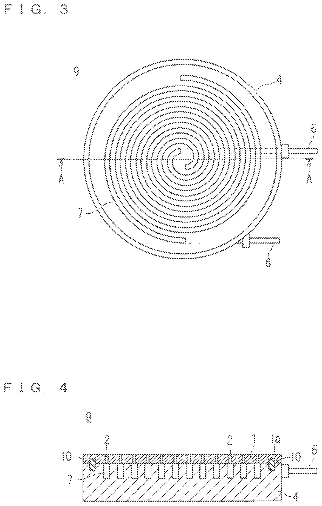
A semiconductor test apparatus includes a chuck top on which a semiconductor wafer is mounted, and contact probes that contact measurement points of semiconductor chips formed on the semiconductor wafer, the chuck top includes a conductor that contacts a lower surface of the semiconductor wafer, a mounting table arranged below the conductor, and a first vacuum tube and a second vacuum tube connected to the mounting table, the conductor has a plurality of suction holes that are arranged in a spiral form in top view, in the mounting table, a flow pass communicating with the plurality of suction holes and having a spiral form in top view, the first vacuum tube is connected to an inner circumference portion of the flow pass, and the second vacuum tube is connected to an outer circumference portion of the flow pass.

Description

BACKGROUND OF THE INVENTIONField of the Invention[0001]The present disclosure relates to a semiconductor test apparatus and a semiconductor test method.Description of the Background Art[0002]A probe device has been proposed for improving the measurement accuracy and power consumption efficiency of electrical characteristic inspection for a power device (corresponding to a semiconductor wafer) having electrodes on both sides of a semiconductor substrate by materializing the reduction in contact resistance and uniformity of contact resistance between a rear side electrode of a semiconductor substrate and the mounting surface conductor of the chuck top on which the semiconductor substrate is mounted (see, for example, Japanese Patent Application Laid-Open No. 2015-26765).[0003]However, in the technique described in Japanese Patent Application Laid-Open No. 2015-26765, a semiconductor wafer is sucked through the vacuum passage; therefore, the pressure loss increases in proportion to the...

Claims


Application Information

Patent Timeline
IPC IPC(8): G01R1/073G01R31/26H01L21/66G01R31/28
CPCG01R1/07342G01R31/2886H01L22/30G01R31/2601H01L22/14
Inventor UEDA, YOSHIYUKINOGUCHI, TAKAYA
Owner MITSUBISHI ELECTRIC CORP
Learn More