
Method and apparatus for growing silicon single crystal ingot

a silicon single crystal and ingot technology, applied in the direction of crystal growth process, polycrystalline material growth, instruments, etc., can solve the problems of reducing the manufacturing affecting the yield and the edge of silicon single crystal ingots other than the facet should be removed,

Pending Publication Date: 2022-08-11
SK SILTRON CO LTD
View PDF1 Cites 0 Cited by
  • Summary
  • Abstract
  • Description
  • Claims
  • Application Information

AI Technical Summary

Benefits of technology

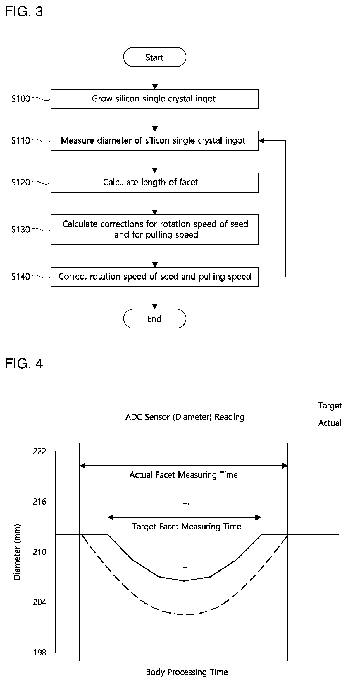
The patent describes a method for growing silicon single crystals. By calculating the length of the facet (the part of the crystal that is shaped like a triangle) using a special formula, the speed of rotation and pulling of the crystal can be maintained without change. When the difference between the calculated facet length and the desired length is detected to be within 5 mm, no adjustments are necessary. When the difference is greater than 5 mm, the rotation speed of the seed (the starting point of the crystal) is reduced by a specific factor. When the difference is smaller than 5 mm, the rotation speed of the seed is increased by a specific factor. The pulling speed of the crystal is also adjusted based on the difference in facet length. By implementing this method, the quality and consistency of the grown silicon single crystals can be improved.

Problems solved by technology

Here, a problem may occur in that an edge of the silicon single crystal ingot other than the facet should be removed by grinding after growth.
Then, the diameter of the ingot determined to be decreased may be transmitted to the AGC and ATC logic, which may cause an error in the pulling speed of the silicon single crystal ingot.
The above-described error causes a problem in that the diameter of the growing silicon single crystal ingot is varied and a body region thereof may be reduced, thereby reducing the manufacturing yield of the silicon single crystal ingot.

Method used


Image

  • Method and apparatus for growing silicon single crystal ingot
  • Method and apparatus for growing silicon single crystal ingot
  • Method and apparatus for growing silicon single crystal ingot

Examples


Embodiment Construction

[0034]Hereinafter, embodiments of the present invention will be described in detail with reference to the accompanying drawings.

[0035]The embodiments of the present invention may be modified into various forms, and the scope of the present invention should not be construed as being limited to the following embodiments. These embodiments are provided so that this disclosure will be thorough and complete, and will fully convey the scope of the disclosure to those skilled in the art.

[0036]In addition, relative terms such as, for example, “first”, “second”, “on” / “upper” / “above”, and “beneath” / “lower” / “below”, used in the following description may be used to distinguish any one substance or element from another substance or element without requiring or containing any physical or logical relationship or sequence between these substances or elements.

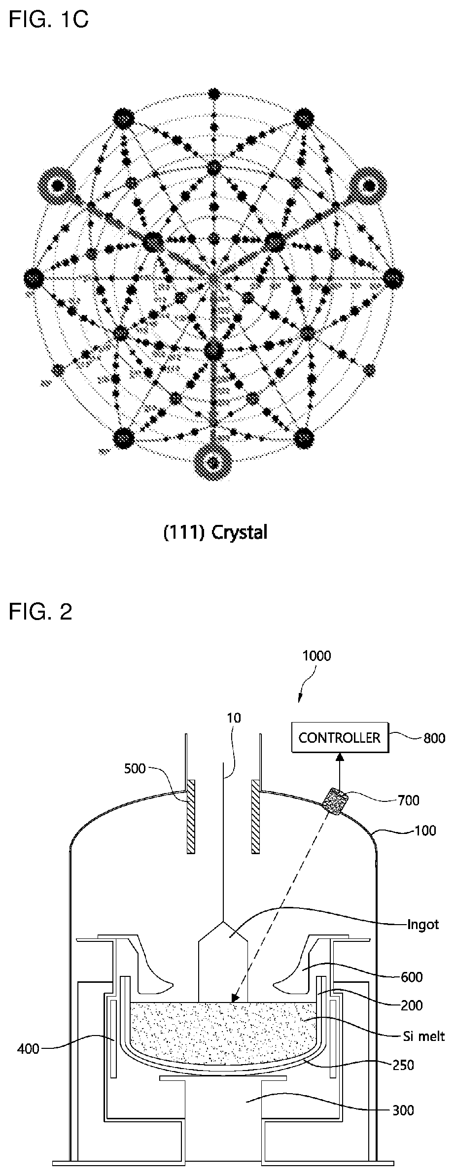
[0037]FIG. 2 illustrates an embodiment of an apparatus for growing a silicon single crystal ingot.

[0038]An apparatus 1000 for growing a silico...


PUM


Abstract

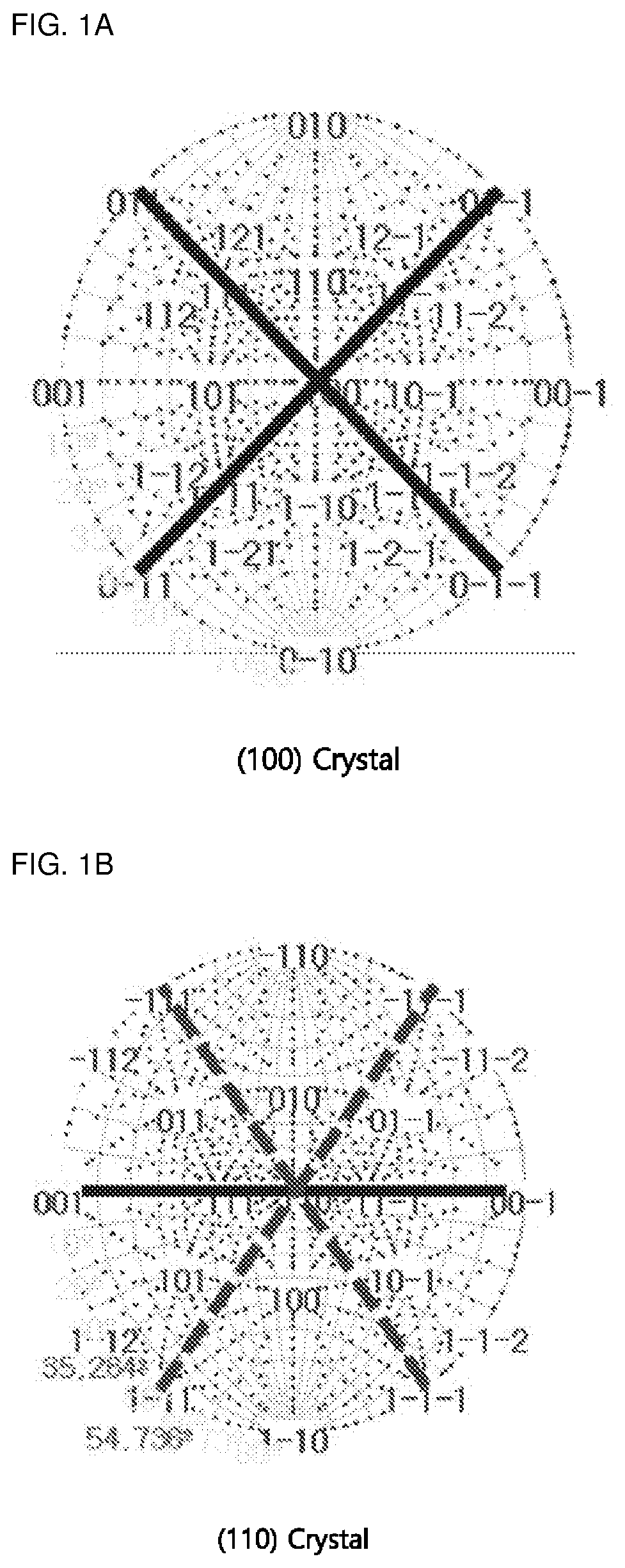
Embodiments provide a method of growing a silicon single crystal ingot, the method including growing a silicon single crystal ingot having crystal orientation of (111) using the Czochralski method, measuring a diameter of the silicon single crystal ingot, calculating a length of a facet of the silicon single crystal ingot, calculating a correction formula for a rotation speed of a seed and a correction formula for a pulling speed of the silicon single crystal ingot based on the calculated facet length, and correcting the rotation speed of the seed and the pulling speed of the silicon single crystal ingot based on a result of the calculation.

Description

[0001]This application claims the benefit of Korean Patent Application No. 10-2021-0018275, filed on Feb. 9, 2021, which is hereby incorporated by reference as if fully set forth herein.BACKGROUND OF THE INVENTIONField of the Invention[0002]Embodiments relate to growth of a silicon single crystal ingot, and more particularly, the embodiments are intended to control a difference between a facet length and a target diameter that occurs while growing a silicon single crystal ingot having crystal orientation of (111).Discussion of the Related Art[0003]A general silicon wafer is manufactured through processes of growing a silicon single crystal to prepare a single crystal (ingot), slicing the single crystal to obtain thin disk-shaped wafers, lapping the wafer to remove damage remaining on the wafer due to mechanical processing of the slicing, polishing the wafer, and cleaning to mirror-polish the polished wafer and remove abrasives or foreign substances attached to the wafer.[0004]In the...

Claims


Application Information

Patent Timeline
IPC IPC(8): C30B15/22C30B29/06C30B15/36C30B15/14C30B15/10
CPCC30B15/22C30B29/06C30B15/10C30B15/14C30B15/36C30B15/00G01B21/10
Inventor HWANG, HYUN JUKIM, SANG HEEPARK, KYUNG TAE
Owner SK SILTRON CO LTD
Learn More