Electronic device including vapor chamber

a technology of electronic devices and vapor chambers, applied in the construction details of electrical apparatuses, instruments, substation equipment, etc., can solve the problems of inconvenient use, inconvenient use, and inability to meet the needs of users, so as to suppress the decrease in rigidity of electronic devices, improve the bonding structure, and strengthen mechanical strength

Pending Publication Date: 2022-08-25
SAMSUNG ELECTRONICS CO LTD
View PDF3 Cites 1 Cited by
  • Summary
  • Abstract
  • Description
  • Claims
  • Application Information

AI Technical Summary

Benefits of technology

This patent describes an electronic device with a vapor chamber that can make the device thinner and more flexible. The vapor chamber is attached to a support member using a strong bond, which helps maintain the device's strength and prevents it from getting bent or change in shape. The plates in the vapor chamber are made stronger through a process like stamping, which helps reinforce the device's mechanical integrity. Overall, this invention makes the device slimmer and stronger, while also reducing manufacturing costs.

Problems solved by technology

Such high-temperature heat may cause malfunction of the electronic device and may cause discomfort to a user.
However, since the vapor chamber is configured to have a relatively large volume through a bonding structure of the two plates, the vapor chamber may act counter to the slimming of the electronic device.
In addition, since pillars are formed on the metal plate through a chemical process (e.g., an etching process), corrosion, perforation, or cracking may occur in the metal plate having a predetermined thickness or less.

Method used


Image

  • Electronic device including vapor chamber
  • Electronic device including vapor chamber
  • Electronic device including vapor chamber

Examples


Embodiment Construction

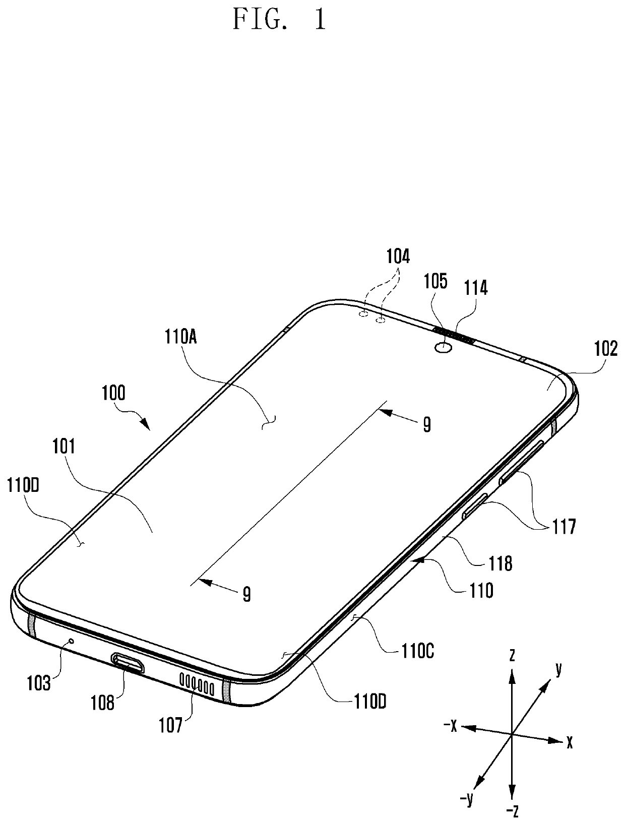
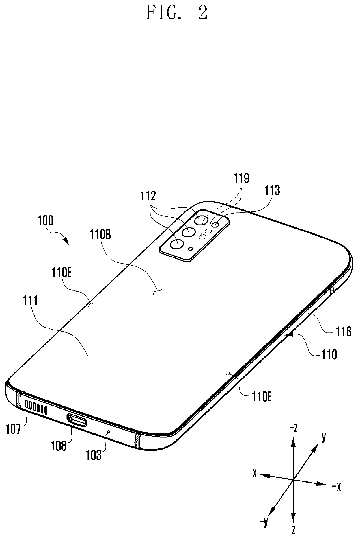
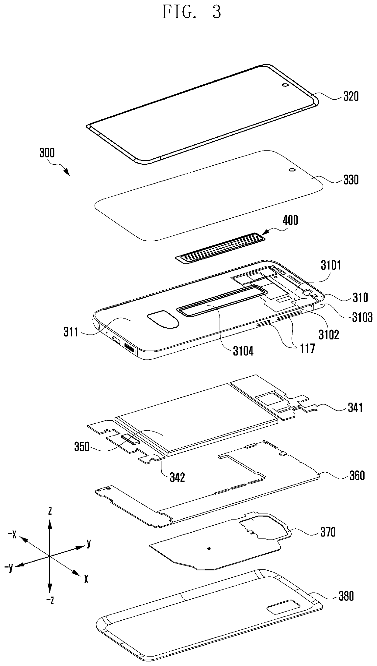
[0023]FIG. 1 is a perspective view illustrating a front surface of a mobile electronic device according to various embodiments, and FIG. 2 is a rear a perspective view illustrating a rear surface of the mobile electronic device shown in FIG. 1 according to various embodiments.

[0024]Referring to FIGS. 1 and 2, a mobile electronic device 100 may include a housing 110 that includes a first surface (or front surface) 110A, a second surface (or rear surface) 110B, and a lateral surface 110C that surrounds a space between the first surface 110A and the second surface 110B. The housing 110 may refer to a structure that forms a part of the first surface 110A, the second surface 110B, and the lateral surface 110C. The first surface 110A may be formed of a front plate 102 (e.g., a glass plate or polymer plate coated with a variety of coating layers) at least a part of which is substantially transparent. The second surface 110B may be formed of a rear plate 111 which is substantially opaque. T...


PUM


Abstract

An electronic device may include: a housing, a support member disposed in an internal space of the housing and including a first surface and a second surface facing a direction opposite the first surface, wherein the support member includes a through hole in at least a portion thereof, and a vapor chamber disposed through at least a portion of the through-hole, wherein the vapor chamber may include: a first plate including a first plate portion including a plurality of pillars and a first flange portion extending along an edge of the first plate portion to have a first width, a second plate having a size corresponding to the first plate portion and including a second plate portion including a recess and a second flange portion extending along an edge of the second plate portion to have a second width less than the first width, and at least one wick disposed in the recess, wherein the wick may be accommodated through a closed space defined through coupling of the first plate and the second plate.

Description

CROSS-REFERENCE TO RELATED APPLICATIONS[0001]This application is a continuation of International Application No. PCT / KR2022 / 001507 designating the United States, filed on Jan. 27, 2022, in the Korean Intellectual Property Receiving Office and claiming priority to Korean Patent Application No. 10-2021-0023220, filed on Feb. 22, 2021, in the Korean Intellectual Property Office, the disclosures of which are incorporated by reference herein in their entireties.BACKGROUNDField[0002]The disclosure relates to an electronic device including a vapor chamber.Description of Related Art[0003]While electronic devices are gradually becoming smaller, functions thereof are gradually being diversified. According to the miniaturization and slimming of electronic devices, electrical elements embedded in an electronic device may be arranged such that the distances of the electronic elements from a surrounding structure are reduced or the electronic elements are concentrated, and may generate high-tempe...

Claims


Application Information

Patent Timeline
IPC IPC(8): H05K7/20
CPCH05K7/20327H05K7/20336H05K7/2099H05K7/20963H04M1/026G06F1/203G06F2200/201G06F1/1626H04M1/02H04M1/0262H04M1/0266H05K5/0017H05K5/0086H05K7/20472
Inventor MOON, HONGKIKOO, KYUNGHAPARK, YOONSUNYOU, YOUNGJAELEE, HYUNJOOAHN, JOSEPH
Owner SAMSUNG ELECTRONICS CO LTD
Why Eureka
Try Eureka