A kind of semiconductor packaging structure and preparation method thereof

A packaging structure and semiconductor technology, applied in semiconductor/solid-state device manufacturing, semiconductor devices, semiconductor/solid-state device components, etc., can solve problems such as pad stripping, hidden dangers in semiconductor chip performance, and reduce semiconductor chip packaging yield, etc., to achieve The effect of avoiding pad peeling and good mechanical characteristics

Active Publication Date: 2017-12-29
SEMICON MFG INT (SHANGHAI) CORP
View PDF1 Cites 0 Cited by
  • Summary
  • Abstract
  • Description
  • Claims
  • Application Information

AI Technical Summary

Problems solved by technology

[0007] However, it is found in actual operation that regardless of the single layer (generally using TaN layer, which has a strong ability to prevent copper-aluminum diffusion) or the multi-layer metal shielding layer structure, the metal shielding layer has the same effect on the ability to prevent copper-aluminum diffusion. It is proportional to the thickness (the current TaN layer is generally about 700A), but too thick TaN is connected to the interconnection metal in the wire bonding strength test, and the pad peeling phenomenon often occurs, which greatly reduces the yield of semiconductor chip packaging. , and cause performance problems for subsequent packaged semiconductor chips

Method used


Image

  • A kind of semiconductor packaging structure and preparation method thereof
  • A kind of semiconductor packaging structure and preparation method thereof
  • A kind of semiconductor packaging structure and preparation method thereof

Examples


Embodiment 1

[0044] refer to Figure 1 to Figure 5 As shown, the specific process of the preparation method of a semiconductor package structure provided by the present invention includes:

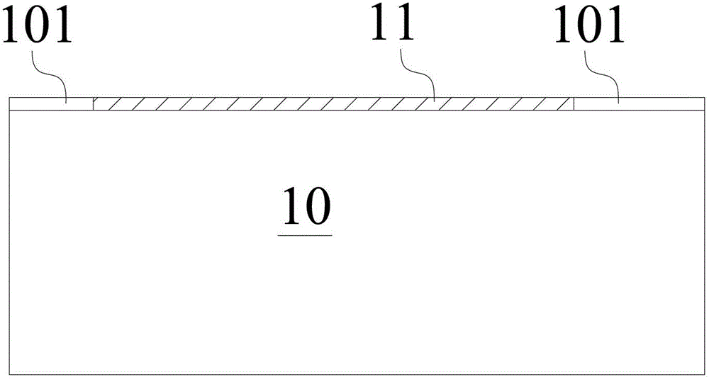
[0045] combined reference figure 1 As shown, a semiconductor substrate 10 is provided. The semiconductor substrate 10 has completed the front-end process in the semiconductor manufacturing process and has formed effective devices, which are collectively referred to as the semiconductor substrate 10 herein. A copper interconnection layer 11 and a dielectric 101 around the copper interconnection layer 11 are formed on the semiconductor substrate 10 . The process for forming the copper interconnection layer is the Dua-Damascene technology, which will not be repeated here.

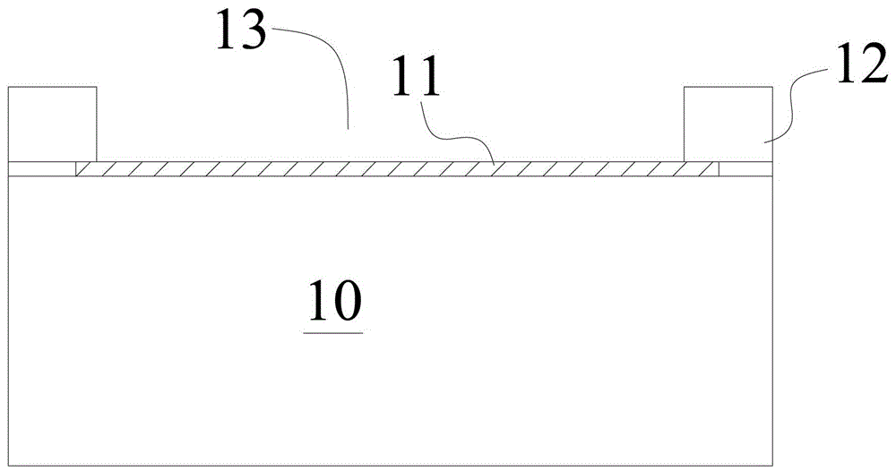
[0046] combined reference figure 2 As shown, thereafter, a passivation layer 12 is deposited on the copper interconnection layer 11 to cover the copper interconnection layer 11; the passivation layer 12 is patterned to form an ope...

Embodiment 2

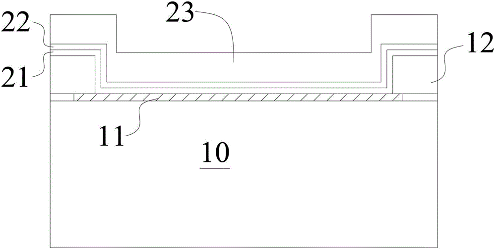
[0058] The technical scheme of this embodiment and embodiment 1 is roughly the same, in conjunction with reference Image 6 , the difference is only that: in the process of preparing the semiconductor package structure in the above-mentioned embodiment 1, after the Ti layer 21 is formed, a TiN layer 24 is deposited on the Ti layer 21 by PVD method. Then the TaN layer 22 is deposited on the TiN layer 24 to form a metal shielding layer with a three-layer stacked structure.

[0059] combined reference Figure 7 with Figure 8 As shown, after the aluminum layer 23 is formed on the TaN layer 22, the aluminum layer 23 is patterned, and the parts on both sides of the aluminum layer 23 are removed by a dry etching process to expose the passivation layer 12, An auxiliary passivation layer 14 is deposited on the passivation layer 12 , and the auxiliary passivation layer 14 is patterned to form an opening 15 exposing the aluminum layer 23 .

[0060] At this time, in the semiconductor ...

Embodiment 3

[0064] This embodiment is roughly the same as the technical solutions of the above-mentioned embodiment 1 and embodiment 2, combined with reference image 3 , Image 6 as well as Figure 9 ~ Figure 11 , the difference being that, in the above image 3 or Image 6After the pad layer 23 is deposited, one or more auxiliary metal shielding layers are deposited on the pad layer 23, and another pad layer 33 is deposited on the one or more auxiliary metal shielding layers. . Afterwards, similar to the above-mentioned process of patterning the pad layer 23, the pad layer 33 is patterned, and the pad layer 33 and the auxiliary metal shields below the pad layer 33 are etched through an etching process. layer and the two sides of the metal shielding layer in a multilayer stacked structure until the passivation layer 12 is exposed. An auxiliary passivation layer 16 is deposited on the pad layer 33 and the passivation layer 12, and the auxiliary passivation layer 16 is patterned to fo...


PUM

PropertyMeasurementUnit
thicknessaaaaaaaaaa
thicknessaaaaaaaaaa

Abstract

The invention provides a semiconductor package structure and a preparation method thereof. The semiconductor package structure includes: a metal interconnection layer on a semiconductor substrate; a metal shielding layer on the metal interconnection layer; a pad layer on the metal shielding layer; the metal shielding layer is a multilayer A superimposed structure, the coefficients of thermal expansion of each layer in the multi-layer superimposed structure decrease gradually from bottom to top. The semiconductor packaging structure has good thermodynamic properties, which can effectively reduce the difference in volume change of the metal interconnect layer and the metal shielding layers caused by thermal expansion and contraction after the annealing process of the semiconductor packaging structure preparation, and thus The probability of cracking at the crystalline interface of each layer caused by it, so as to avoid the phenomenon of pad peeling. Moreover, the metal shielding layer of the multi-layer stacked structure has better mechanical properties, which can alleviate the damage to the active area of ​​the semiconductor device caused by various stresses generated by the welding and wire bonding process.

Description

technical field [0001] The invention relates to the field of semiconductor preparation, in particular to a semiconductor packaging structure and a preparation method thereof. Background technique [0002] With the continuous improvement of semiconductor manufacturing technology and the continuous reduction of gate size in transistors, the size of integrated circuit devices is continuously reduced, and a large number of semiconductor elements are densely embedded in the chip substrate with a multi-layer interconnection structure, and through multi-layer Metal interconnect layer connection. In the existing semiconductor technology, copper is the most commonly used wiring for metal interconnection layers due to its good electrical conductivity. For specific technology, please refer to the Chinese patent application with publication number CN1881557A. [0003] In the back end of line (BEOL) of semiconductor device fabrication, welding and wire bonding technology is a widely use...

Claims


Application Information

Patent Timeline
Patent Type & Authority Patents(China)
IPC IPC(8): H01L21/768H01L21/60H01L23/532H01L23/488
CPCH01L24/05H01L2224/02166H01L2224/05556H01L2924/351
Inventor 杨志刚陈林林
Owner SEMICON MFG INT (SHANGHAI) CORP
Why Eureka
Try Eureka