

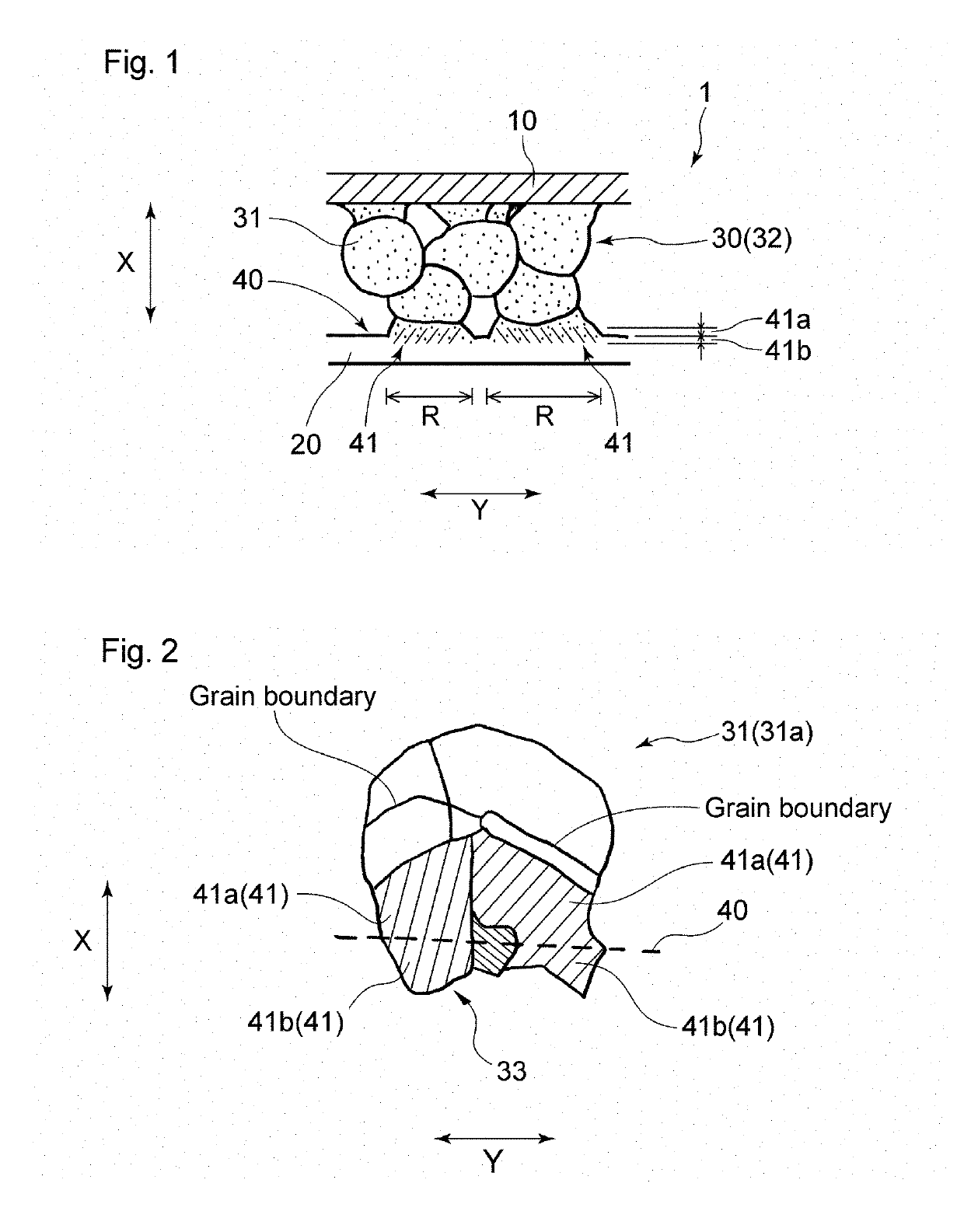
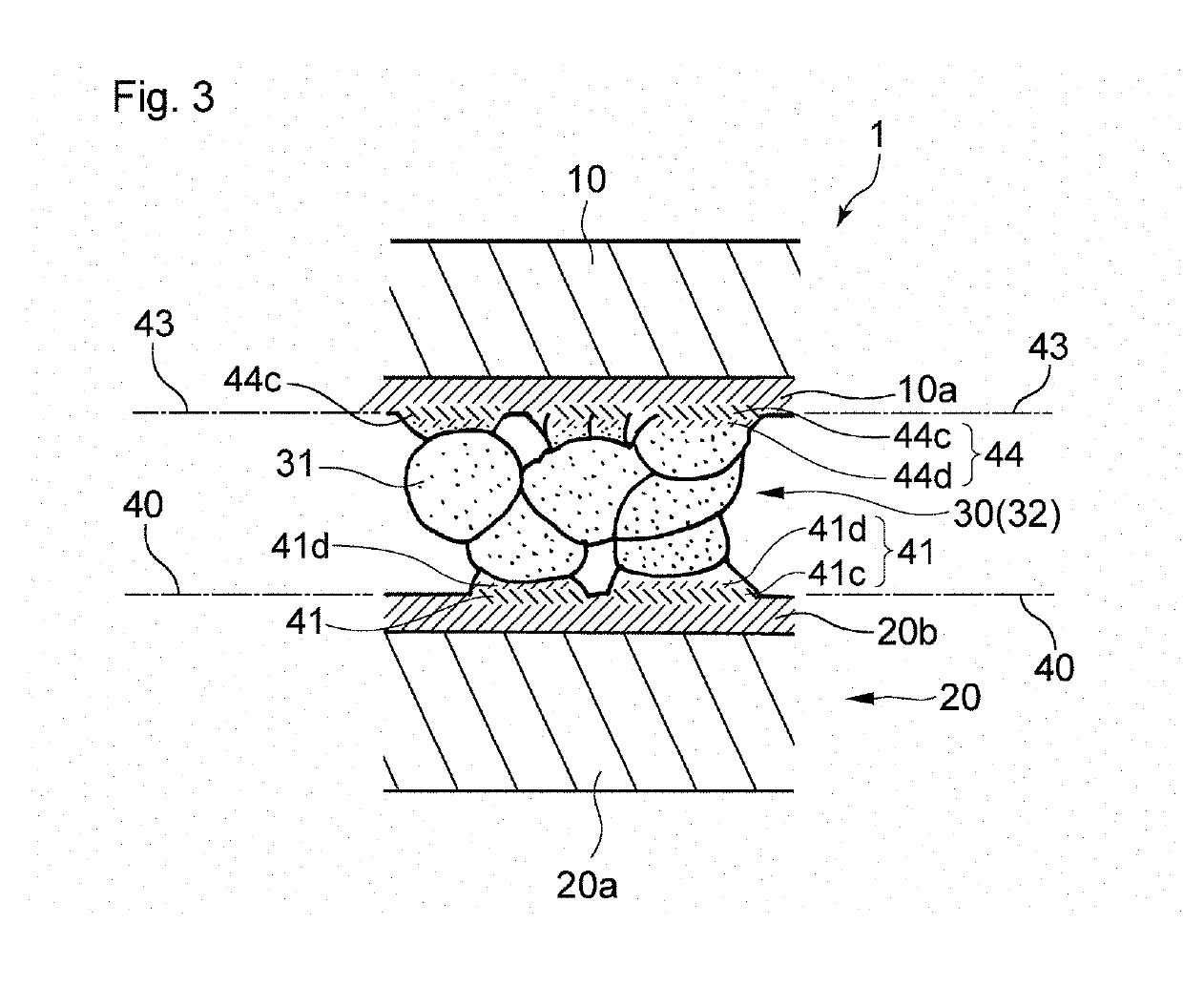
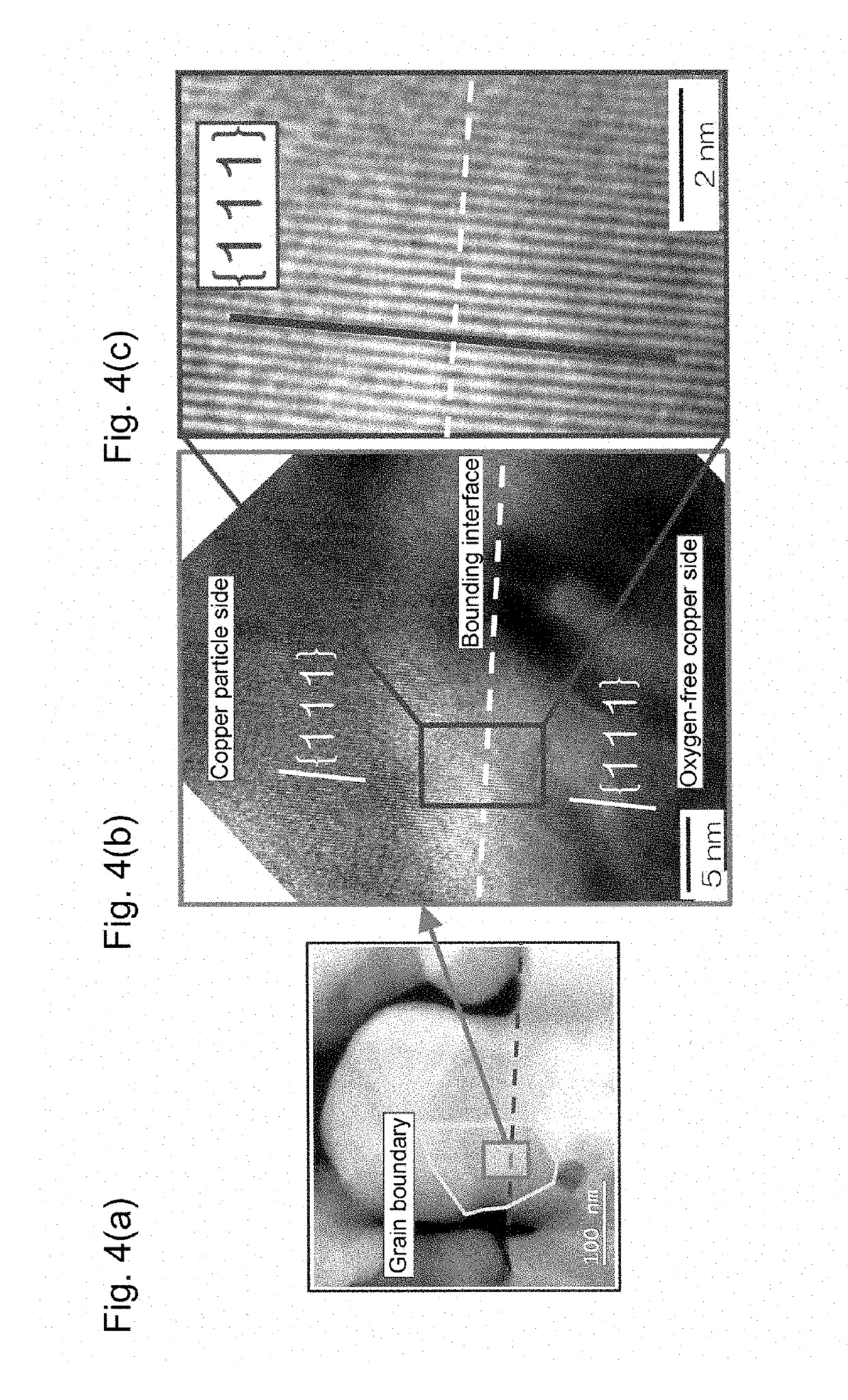
Bonding junction structure
a junction structure and bonding technology, applied in solid-state devices, basic electric elements, chemistry apparatuses and processes, etc., can solve the problems of large amount of etc., to prevent damage to semiconductor devices caused by generated heat generation, reduce power loss in inverters and converters, and improve equipment energy utilization efficiency
- Summary
- Abstract
- Description
- Claims
- Application Information
AI Technical Summary
Benefits of technology
Problems solved by technology
Method used
Image

Examples
example 1
[0095]In the present example, a die bonding joining structure having the structure shown in FIG. 1 was produced.
(1) Production of Copper Powder and Copper Paste
[0096]A 500-ml round-bottomed flask provided with a stirring blade was prepared. As a copper source, 15.71 g of copper acetate monohydrate was put into this round-bottomed flask. Furthermore, 10 g of water and 70.65 g of isopropanol serving as an organic solvent were put into this round-bottomed flask to obtain a reaction mixture. This reaction mixture was heated to 60° C. while being stirred at 150 rpm. While stirring was continued, 1.97 g of hydrazine monohydrate was added to the reaction mixture all at once. Then, the reaction mixture was stirred for 30 minutes. After that, 17.73 g of hydrazine monohydrate was added to the reaction mixture. The reaction mixture was further stirred for 30 minutes. After that, 7.88 g of hydrazine monohydrate was added to the reaction mixture. Then, the reaction mixture was continuously stirr...
example 2
[0105]In the present example, a die bonding joining structure having the structure shown in FIG. 3 was produced.
(1) Production of Copper Powder and Copper Paste
[0106]A copper powder was obtained in the same manner as in Example 1 except that the amount of isopropanol used was 39.24 g, and the amount of water used was 50 g. With respect to this copper powder, the average particle diameter D was 0.24 μm, the BET specific surface area (SSA) was 3.17 m2 / g, DBET was 0.21 μm, D / DBET was 1.2, the total content of C, P, Si, Ti, and Zr was 0.04%, the copper content was more than 99.8%, the crystallite diameter was 35 nm, and the sintering onset temperature was 170° C. This copper powder was mixed with a copper powder composed of copper particles formed through wet synthesis, namely, CS-20 (trade name) manufactured by Mitsui Mining & Smelting Co., Ltd. in a mass ratio of 56:44 to obtain a mixed copper powder. After that, the procedure was performed in the same manner as in Example 1, and thus...
example 3
[0119]In the present example, a die bonding joining structure composed of nickel and having the structure shown in FIG. 1 was produced.
(1) Production of Nickel Paste
[0120]A nickel powder NN-20 manufactured by Mitsui Mining & Smelting Co., Ltd. was used. The average particle diameter D of primary particles of this nickel powder was 20 nm. A nickel paste was obtained by kneading 85 parts of this nickel powder and 15 parts of triethanolamine (manufactured by Kanto Chemical Co., Inc.) using a triple roll mill.
(2) Production of Die Bonding Joining Structure
[0121]The nickel paste was applied to a support formed of a 15-mm-square nickel plate (99.98% purity) with a thickness of 0.1 mm through screen printing using a metal mask with a thickness of 50 μm such that the applied nickel paste was formed into a shape 10 mm square. A 10-mm-square nickel plate (99.98% purity) with a thickness of 0.1 mm was placed on the center of the support as a die. The temperature was increased to 300° C. at a r...
PUM
| Property | Measurement | Unit |
|---|---|---|
| traverse length | aaaaa | aaaaa |
| length | aaaaa | aaaaa |
| length | aaaaa | aaaaa |
Abstract
Description
Claims
Application Information