Wafer far edge temperature measurement system with lamp bank alignment

a technology of far edge temperature and measurement system, which is applied in the direction of optical radiation measurement, instruments, crystal growth process, etc., can solve the problems of undesirable crystallographic slip, uniform temperature distribution of the lamp bank, and uneven physical properties of the film over the substrate surface, etc., to achieve accurate and repeatable measurement

Pending Publication Date: 2022-09-22
ASM IP HLDG BV
View PDF0 Cites 0 Cited by
  • Summary
  • Abstract
  • Description
  • Claims
  • Application Information

AI Technical Summary

Benefits of technology

[0009]Disclosed herein, according to various embodiments, is a reactor system or apparatus for use in semiconductor processing such as chemical vapor deposition (CVD) and other deposition steps. The reactor system is designed to provide accurate monitoring of substrate (e.g., a wafer) temperatures during deposition steps. More specifically, the reactor system includes a pyrometer mounting assembly adapted to support and position three or more pyrometers (e.g., infrared (IR) pyrometers) relative to the reaction chamber to measure a center wafer temperature and a wafer edge temperature as well as reaction chamber temperature. The pyrometer mounting assembly is configured to provide a small spot size (or temperature sensing area) with the edge pyrometer to assist in far-edge wafer temperature measurement.
[0010]Additionally, a jig assembly, and associated assembly method, is provided for use in achieving accurate alignment of the IR pyrometer sensing spot (or the edge pyrometer) relative to the wafer, when the pyrometer mounting assembly is mounted upon a lamp bank in the reactor system or in each tool setup. The wafer far edge temperature sensing techniques described herein ensure the accurate and repeatable measurement of wafer temperatures and associated process control using monitored temperatures.

Problems solved by technology

One problem, though, with use of radiant heat is that, in some reactors, the lamps can create nonuniform temperature distributions on the substrate surface, such as localized hot spots, due to the localized nature of the lamps, focusing effects, and interference effects.
If the temperature varies across the surface of the substrate, uneven deposition of the film may occur and the physical properties in the film may not be uniform over the substrate surface.
Furthermore, in epitaxial deposition, even slight temperature nonuniformity can result in undesirable crystallographic slip.
If a CVD process or other deposition step produces deposited layers with nonuniformities, semiconductor devices formed on different die may have inconsistent operational characteristics or may fail altogether.
If such a temperature gradient is large enough, it will greatly impact the quality of a grown epitaxial film such as by producing slip defects and achieving poor thickness or resistivity uniformity.

Method used


Image

  • Wafer far edge temperature measurement system with lamp bank alignment
  • Wafer far edge temperature measurement system with lamp bank alignment
  • Wafer far edge temperature measurement system with lamp bank alignment

Examples


Embodiment Construction

[0032]Although certain embodiments and examples are disclosed below, it will be understood by those in the art that the disclosure extends beyond the specifically disclosed embodiments and / or uses of the disclosure and obvious modifications and equivalents thereof. Thus, it is intended that the scope of the disclosure should not be limited by the particular embodiments described herein.

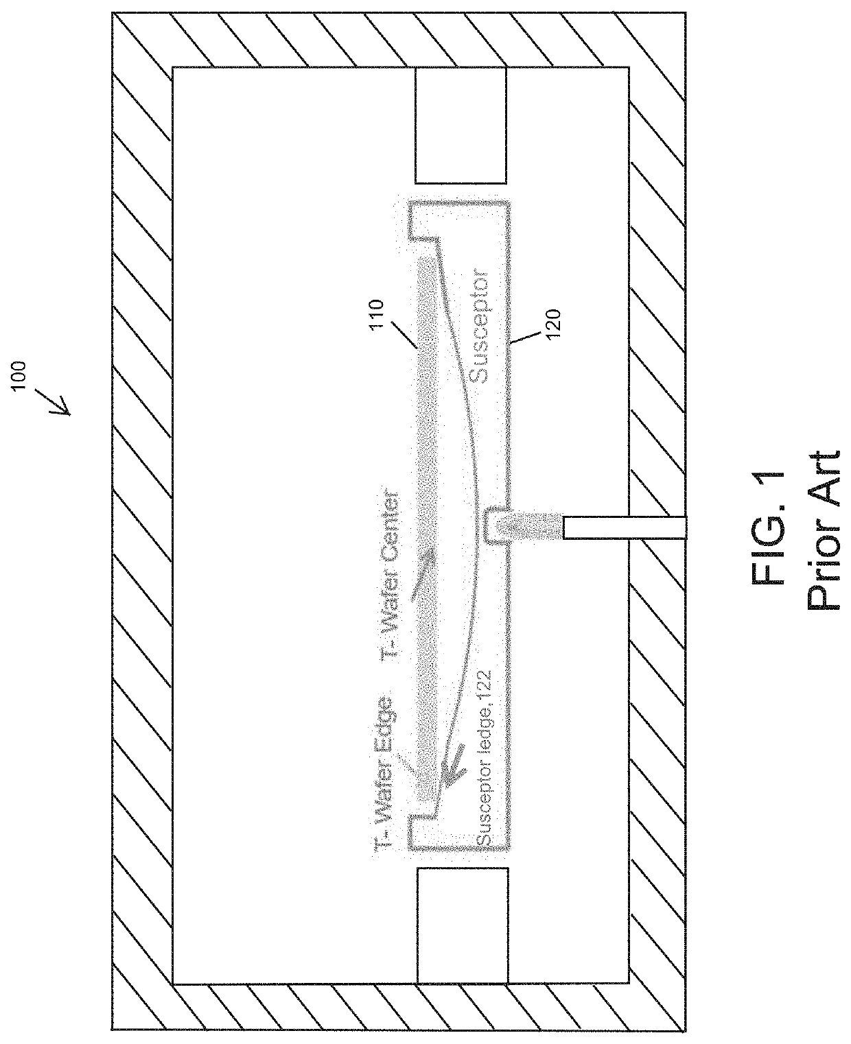
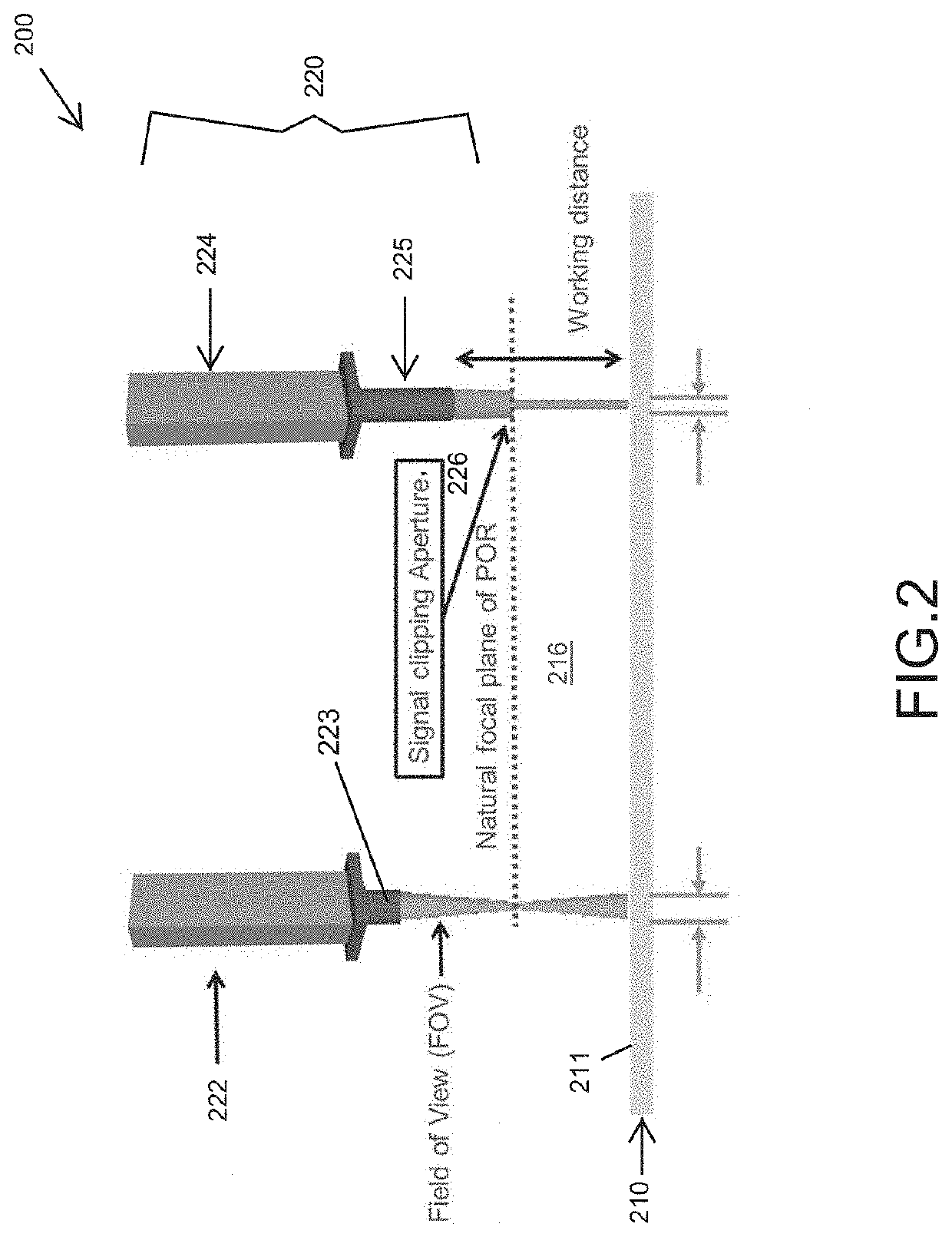
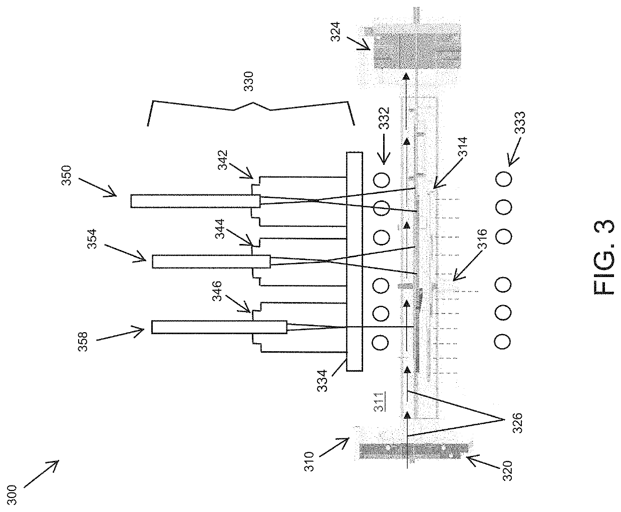
[0033]The illustrations presented herein are not meant to be actual views of any particular material, apparatus, structure, or device, but are merely representations that are used to describe embodiments of the disclosure.

[0034]As used herein, the terms “wafer” and “substrate” may be used interchangeably to refer to any underlying material or materials that may be used, or upon which, a device, a circuit, or a film may be formed.

[0035]As used herein, the term “chemical vapor deposition” (CVD) may refer to any process wherein a substrate is exposed to one or more volatile precursors, which react and / or...


PUM

PropertyMeasurementUnit
distanceaaaaaaaaaa
outer diameteraaaaaaaaaa
temperaturesaaaaaaaaaa

Abstract

A reactor system designed to provide accurate monitoring of wafer temperatures during deposition steps. The reactor system includes a pyrometer mounting assembly supporting and positioning three or more pyrometers (e.g., infrared (IR) pyrometers) relative to the reaction chamber to measure a center wafer temperature and an edge wafer temperature as well as reaction chamber temperature. The pyrometer mounting assembly provides a small spot size or temperature sensing area with the edge pyrometer to accurately measure edge wafer temperatures. A jig assembly, and installation method for each tool setup, is provided for use in achieving accurate alignment of the IR pyrometer sensing spot (and the edge pyrometer) relative to the wafer, when the pyrometer mounting assembly is mounted upon a lamp bank in the reactor system or in tool setup. The wafer edge temperature sensing with the reactor system assembled with proper alignment ensures accurate and repeatable measurement of wafer temperatures.

Description

CROSS-REFERENCE TO RELATE APPLICATIONS[0001]This application claims priority to and the benefit of U.S. Provisional Patent Application No. 63 / 162,878, filed Mar. 18, 2021 and entitled “FILM DEPOSITION SYSTEMS AND METHODS,” and U.S. Provisional Patent Application No. 63 / 270,668, filed Oct. 22, 2021 and entitled “WAFER FAR EDGE TEMPERATURE MEASUREMENT SYSTEM WITH LAMP BANK ALIGNMENT,” which are hereby incorporated by reference herein to the extent that they do not conflict with the present disclosure.FIELD OF THE DISCLOSURE[0002]The present disclosure relates generally to methods and systems for monitoring wafer temperatures in a semiconductor processing or reactor system, and, more particularly, to methods and apparatus for monitoring far edge temperatures of wafers in semiconductor processing or reactor systems, with a design to ensure accurate assembly of a reactor system including accurate, repeatable placement of its lamp bank for edge temperature monitoring.BACKGROUND OF THE DIS...

Claims


Application Information

Patent Timeline
Patent Type & Authority Applications(United States)
IPC IPC(8): H01L21/67H05B31/00
CPCH01L21/67248H05B31/0081G01J5/0806G01J5/0007G01J5/0205C23C16/52H01L21/67115G01J5/084G01J5/0846G01J5/026H01L21/68C30B25/105C30B25/08C23C16/46
Inventor NAIK, RUTVIJHUANG, SHUJINSU, JUNWEILIN, XING
Owner ASM IP HLDG BV
Why Eureka
Try Eureka