Manufacturing method of semiconductor device

Pending Publication Date: 2022-09-22
MITSUBISHI ELECTRIC CORP
0 Cites 0 Cited by

AI-Extracted Technical Summary

Problems solved by technology

In a module using a SiC MOSFET, a plurality of chips need to be connected in parallel to increase current capacity, because an area of the SiC MOSFET is difficult to be increased.
However, there is a problem that dust is generated in grinding process, and moisture enters from a ground surface in a cas...

Method used

[0030]The control electrode 6 of each of the plurality of semiconductor chips 1 is connected to the first electrode 8 of the wiring chip 2 with a connection member 16. The connection member 16 is, for example, a wire formed with gold, silver or aluminum. It is possible to reduce a dimension of the control electrode 6 of the semiconductor chip 1 by using a small-diameter wire formed with gold or silver. It is therefore possible to increase an effective area and reduce manufacturing cost of the semiconductor chip 1.
[0040]In contrast, in the present embodiment, even if the heights of the control electrode member 14 and the main electrode member 12 vary and a gap is generated between the main electrode member 12 and the mold 18 and between the control electrode member 14 and the mold 18, the buffer material 19 fills the gap. Thus, the distal end surfaces of the main electrode member 12 and the control electrode member 14 are exposed without being covered with the sealing material 17 in the sealing process, and thus, the sealing material 17 is not ground after the sealing process. It is therefore possible to reliably lead the electrode members out of the upper surface of the device while preventing increase in manufacturing cost.
[0043]Further, in a case where the semiconductor chip 1 incorporates a temperature sensing device or a current sensing device, these devices are often vulnerable to static electricity compared to a main portion. Thus, a surface of the buffer material 19 which contacts the distal end surfaces of the main electrode member 12 and the control electrode member 14 preferably has conductivity. This prevents occurrence of a potential difference between terminals during and after sealing, so that it is possible to prevent overvoltage breakdown of the semiconductor chip 1 by static electricity.
[0044]FIG. 12 is a cross-sectional view illustrating a modified example of the manufacturing method of the semiconductor device according to the first embodiment. The buffer ...

Benefits of technology

[0006]In the present disclosure, even if the heights of the control electrode member and the main electrode member vary and a gap is generated between the main electrode member and the control electrode member, and the mold, the buffer material fills the gap. Thus, the distal end surfaces of the main electrode member and the co...

Abstract

A semiconductor chip including a main electrode and a control electrode is bonded to a substrate. A wiring chip including a first electrode, a second electrode and a wiring is bonded to the substrate. A main electrode member is bonded to the main electrode. A control electrode member is bonded to the second electrode. The control electrode is bonded to the first electrode with a connection member. The semiconductor chip, the substrate, the wiring chip, the main electrode member, the control electrode member and the connection member are putted into a mold and are sealed with sealing material by injecting the sealing material into the mold in a state that distal end surfaces of the main electrode member and the control electrode member are pressed against a buffer material provided between the main electrode member/the control electrode member and the mold. The sealing material is not ground.

Application Domain

Semiconductor/solid-state device detailsSolid-state devices +2

Technology Topic

PhysicsComposite material +5

Image

  • Manufacturing method of semiconductor device
  • Manufacturing method of semiconductor device
  • Manufacturing method of semiconductor device

Examples

  • Experimental program(2)

Example

First Embodiment
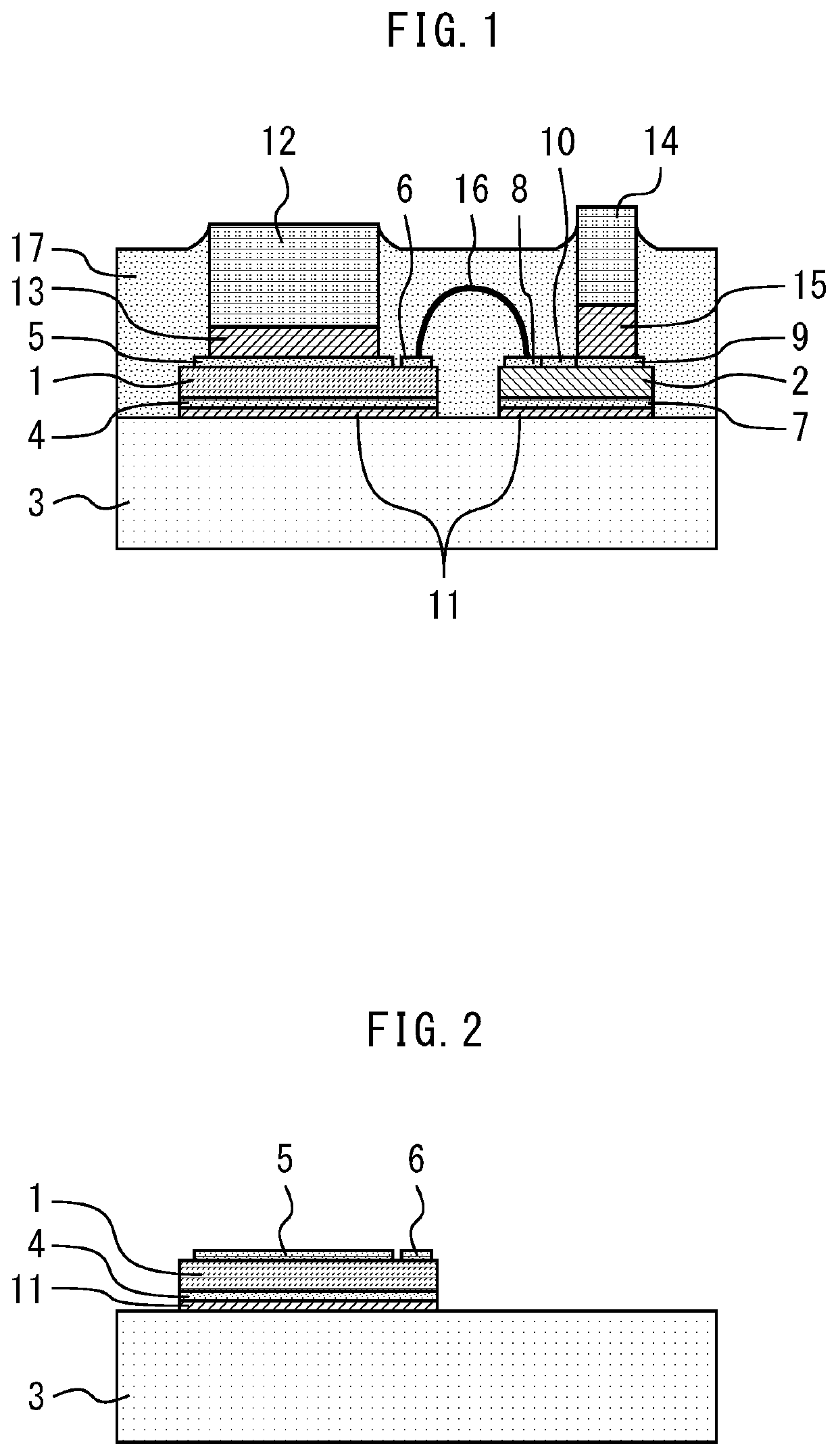
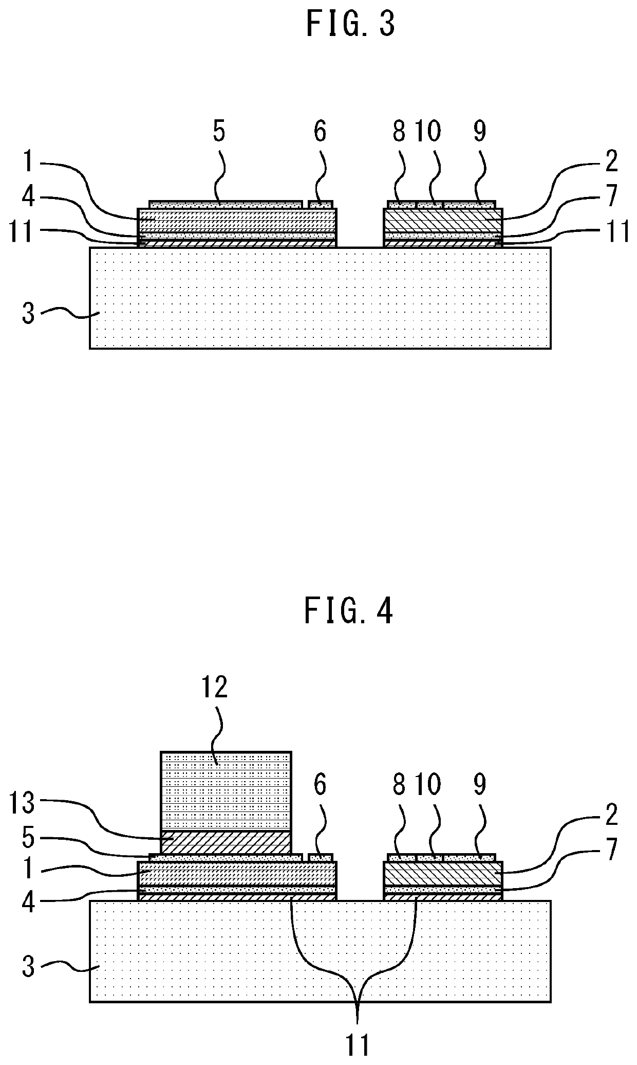
[0025]FIG. 1 is a cross-sectional view illustrating a semiconductor device according to a first embodiment. A plurality of semiconductor chips 1 and one wiring chip 2 are bonded to a substrate 3. The semiconductor chip 1 includes a backside electrode 4 on a back side, and a main electrode 5 and a control electrode 6 on a front side. The semiconductor chip 1 is, for example, a MOSFET. The control electrode 6 is, for example, a gate electrode or a Kelvin source electrode. In a case where the semiconductor chip 1 incorporates a temperature sensing device or a current sensing device, the semiconductor chip 1 further includes control electrodes which respectively correspond to the temperature sensing device and the current sensing device.
[0026]The backside electrode 4 is, for example, a metal film in which a silicide layer, a titanium layer, a nickel layer, a titanium layer and a gold or silver layer are stacked in this order from the semiconductor chip 1 side using a sputtering method. The main electrode 5 and the control electrode 6 are, for example, metal films in which an aluminum layer is formed on the semiconductor chip 1 using a sputtering method, and a nickel layer, a palladium layer and a gold layer are stacked on the aluminum layer using a plating method. Alternatively, the main electrode 5 and the control electrode 6 may be metal films in which an aluminum layer, a titanium layer, a nickel layer, a titanium layer and a gold or silver layer are stacked using a sputtering method. Other than these films, a stacked film having similar functions may be selected.
[0027]The wiring chip 2 includes a bonding layer 7 on a back side, and a first electrode 8, a second electrode 9 and a wiring 10 which connects the first electrode 8 and the second electrode 9 on a front side. The wiring chip 2 is, for example, a device formed with silicon, an insulating film such as an oxide film is formed on an Si surface, and the first electrode 8, the second electrode 9 and the wiring 10 are formed on the insulating film. The first electrode 8, the second electrode 9 and the wiring 10 are, for example, a wiring pattern formed with aluminum. A metal layer which can be bonded is provided on at least the second electrode 9. A similar metal layer may also be provided on the first electrode 8. The metal layer which can be bonded is, for example, a stacked metal film which is similar to the main electrode 5 of the semiconductor chip 1. The bonding layer 7 is, for example, a metal film which is similar to the backside electrode 4 of the semiconductor chip 1. The backside electrode 4 of the semiconductor chip 1 and the bonding layer 7 of the wiring chip 2 are respectively bonded to the substrate 3 via a bonding material 11.
[0028]A main electrode member 12 is bonded to the main electrode 5 of the semiconductor chip 1 via a first bonding material 13. The main electrode member 12 is, for example, formed with copper. In a case where the main electrode member 12 is provided over main electrodes 5 of a plurality of semiconductor chips 1, portions bonded to the main electrodes 5 protrude, and portions which connect the bonded portions are thinner than the portions bonded to the main electrodes 5. This enables the main electrodes 5 of the plurality of semiconductor chips 1 to be connected at the same potential while avoiding a peripheral withstand voltage structure of the semiconductor chip 1. Alternatively, it is also possible to employ a configuration where the main electrodes 5 of the plurality of semiconductor chips 1 are independent of each other, and the main electrodes 5 have the same potential when the main electrodes 5 are connected to an external electrode.
[0029]A control electrode member 14 is bonded to the second electrode 9 of the wiring chip 2 via a second bonding material 15. The control electrode member 14 is, for example, a plurality of blocks formed with copper.
[0030]The control electrode 6 of each of the plurality of semiconductor chips 1 is connected to the first electrode 8 of the wiring chip 2 with a connection member 16. The connection member 16 is, for example, a wire formed with gold, silver or aluminum. It is possible to reduce a dimension of the control electrode 6 of the semiconductor chip 1 by using a small-diameter wire formed with gold or silver. It is therefore possible to increase an effective area and reduce manufacturing cost of the semiconductor chip 1.
[0031]The semiconductor chip 1, an upper surface of the substrate 3, the wiring chip 2, the main electrode member 12, the control electrode member 14 and the connection member 16 are sealed with a sealing material 17. The sealing material 17 is, for example, an epoxy resin mixed with filler. Distal end portions of the main electrode member 12 and the control electrode member 14 protrude from an upper surface of the sealing material 17, and distal end surfaces are exposed from the sealing material 17.
[0032]Subsequently, a manufacturing method of the semiconductor device according to the present embodiment will be described. FIGS. 2 to 7 are cross-sectional views illustrating a manufacturing method of a semiconductor device according to the first embodiment. First, as illustrated in FIG. 2, the semiconductor chip 1 is bonded to the substrate 3. Then, as illustrated in FIG. 3, the wiring chip 2 is bonded to the substrate 3. In this event, the backside electrode 4 of the semiconductor chip 1 and the bonding layer 7 of the wiring chip 2 are respectively bonded to the substrate 3 via the bonding material 11. The bonding material 11 may be, for example, solder, or bonding may be achieved through sinter bonding using a bonding material formed with silver or copper. The sinter bonding may be pressure bonding in which a temperature is increased while the semiconductor chip 1 and the wiring chip 2 are pressed from upper surfaces of the electrodes, or may be pressure-less bonding in which a pressure is not applied. Alternatively, the wiring chip 2 may be bonded using an adhesive agent, or the like, which can obtain thermomechanical stability by being heated. However, in a case where the wiring chip 2 formed with silicon is used, there is a case where the wiring chip 2 breaks, and thus, a bonding method in which a pressure is not applied is preferable.
[0033]Then, as illustrated in FIG. 4, the main electrode member 12 is bonded to the main electrode 5 via the first bonding material 13. Then, as illustrated in FIG. 5, the control electrode member 14 is bonded to the second electrode 9 via the second bonding material 15. The first bonding material 13 and the second bonding material 15 may be, for example, solder, or bonding may be achieved through sinter bonding using a bonding material formed with silver or copper. Although the sinter bonding may be pressure bonding in which a temperature is increased while the electrodes are pressed from upper surfaces of the electrodes, pressure-less bonding in which a pressure is not applied is preferable.
[0034]The thicknesses of the main electrode member 12 and the control electrode member 14 vary due to variation in manufacturing tolerance of the main electrode member 12 and the control electrode member 14. Further, thicknesses of the first bonding material 13 and the second bonding material 15 also vary. Thus, a height of a distal end surface of the bonded main electrode member 12 is different from a height of a distal end surface of the bonded control electrode member 14.
[0035]Then, as illustrated in FIG. 6, the control electrode 6 is bonded to the first electrode 8 with the connection member 16. Then, as illustrated in FIG. 7, a semi-finished product including the semiconductor chip 1, the substrate 3, the wiring chip 2, the main electrode member 12, the control electrode member 14 and the connection member 16, which are bonded, is put into a mold 18. In this event, a buffer material 19 is provided between the main electrode member 12 and the mold 18 and between the control electrode member 14 and the mold 18.
[0036]When the distal end surfaces of the main electrode member 12 and the control electrode member 14 are pressed against the buffer material 19, thicknesses of portions of the buffer material 19, which contact the main electrode member 12 and the control electrode member 14 become thin by pressing force. In a case where the height of the distal end surface of the main electrode member 12 is different from the height of the distal end surface of the control electrode member 14, a thickness of a portion of the buffer material 19, which contacts the main electrode member 12 is different from a thickness of a portion which contacts the control electrode member 14. The semiconductor chip 1, the upper surface of the substrate 3, the wiring chip 2, the main electrode member 12, the control electrode member 14 and the connection member 16 are sealed with the sealing material 17 using a transfer molding sealing method in which the sealing material 17 is injected into the mold 18 in this state.
[0037]The buffer material 19 is removed from the upper surface of the semiconductor device when the semiconductor device is removed from the mold 18 after sealing. Through the above-described process, the semiconductor device in which the distal end surfaces of the main electrode member 12 and the control electrode member 14 are exposed from the sealing material 17 is manufactured without grinding the sealing material 17.
[0038]Further, it is possible to constitute a higher-order semiconductor device such as a half-bridge circuit and a full-bridge circuit by using a plurality of manufactured semiconductor devices. In this case, the substrate 3 is electrically or thermally connected to a drain circuit pattern through solder bonding or sinter bonding. The main electrode member 12 is electrically connected to a source circuit pattern through wire bonding, ribbon bonding or solder bonding of a lead frame. Thereafter, a higher-order semiconductor device is manufactured by covering the periphery of the semiconductor device and the circuit patterns with a secondary sealing material such as gel. Note that in a case where solder is used as a bonding material of the semiconductor chip 1, it is preferable to use solder having a melting point higher than a bonding process temperature when the higher-order semiconductor device is assembled.
[0039]Subsequently, effects of the present embodiment will be described while being compared with a comparative example. FIGS. 8 to 10 are cross-sectional views illustrating a manufacturing method of a semiconductor device according to the comparative example. In the comparative example, as illustrated in FIG. 8, the buffer material 19 is not used in resin sealing process. Thus, a gap is generated between the mold 18 and the main electrode member 12 and between the mold 18 and the control electrode member 14, and the sealing material 17 goes into the gap. Thus, as illustrated in FIG. 9, there is a case where the main electrode member 12 or the control electrode member 14 cannot be exposed from the surface of the sealing material 17. Thus, as illustrated in FIG. 10, it is necessary to grind the extra sealing material 17 and parts of the main electrode member 12 and the control electrode member 14 to expose the main electrode member 12 and the control electrode member 14.
[0040]In contrast, in the present embodiment, even if the heights of the control electrode member 14 and the main electrode member 12 vary and a gap is generated between the main electrode member 12 and the mold 18 and between the control electrode member 14 and the mold 18, the buffer material 19 fills the gap. Thus, the distal end surfaces of the main electrode member 12 and the control electrode member 14 are exposed without being covered with the sealing material 17 in the sealing process, and thus, the sealing material 17 is not ground after the sealing process. It is therefore possible to reliably lead the electrode members out of the upper surface of the device while preventing increase in manufacturing cost.
[0041]FIG. 11 is a cross-sectional view illustrating a distal end portion of the main electrode member after sealing. When the distal end surfaces of the main electrode member 12 and the control electrode member 14 are pressed against the buffer material 19, portions of the buffer material 19, which contact the control electrode member 14 and the main electrode member 12 becomes thinner than a portion which does not contact the control electrode member 14 and the main electrode member 12. The buffer material 19 is gradually thinner from the portion which does not contact the control electrode member 14 and the main electrode member 12 toward the portions which contact the control electrode member 14 and the main electrode member 12. Because resin sealing is performed in this state, a shape of the sealing material 17 follows a shape of the buffer material 19. Thus, the sealing material 17 provided on side surfaces of the distal end portions of the main electrode member 12 and the control electrode member 14 has a tapered shape in which a film thickness in a lateral direction in the figure becomes thinner toward the distal end surfaces of the main electrode member 12 or the control electrode member 14.
[0042]In a case where there is a difference between linear expansion coefficients of the main electrode member 12 and the control electrode member 14 and a linear expansion coefficient of the sealing material 17, stress occurs between both by a cooling/heating cycle, or the like. If a crack is generated in the sealing material 17 or the sealing material 17 peels due to stress, moisture enters upon a moisture resistance test, or the like, and reaches the semiconductor chip 1, or the like, which shortens the life of the semiconductor device. For that, in the present embodiment, the film thickness of the sealing material 17 is gradually thinner toward the distal end surfaces of the main electrode member 12 or the control electrode member 14 as described above. Thus, stress becomes smaller toward end surfaces of the main electrode member 12 or the control electrode member 14, so that it is possible to prevent the sealing material 17 from peeling from the control electrode member 14 and the main electrode member 12.
[0043]Further, in a case where the semiconductor chip 1 incorporates a temperature sensing device or a current sensing device, these devices are often vulnerable to static electricity compared to a main portion. Thus, a surface of the buffer material 19 which contacts the distal end surfaces of the main electrode member 12 and the control electrode member 14 preferably has conductivity. This prevents occurrence of a potential difference between terminals during and after sealing, so that it is possible to prevent overvoltage breakdown of the semiconductor chip 1 by static electricity.
[0044]FIG. 12 is a cross-sectional view illustrating a modified example of the manufacturing method of the semiconductor device according to the first embodiment. The buffer material 19 includes a resin material which does not have conductivity, and a conductive thin film 20 such as a carbon sheet and a metallic foil provided between the resin material and the main electrode member 12 and between the resin material and the control electrode member 14. The distal end surfaces of the main electrode member 12 and the control electrode member 14 contact the conductive thin film 20, and a potential difference does not occur between terminals, so that it is possible to prevent overvoltage breakdown of the semiconductor chip 1 by static electricity. Further, use of the conductive thin film 20 enables use of an inexpensive sealing material 17 such as Teflon. Alternatively, the buffer material 19 may include carbon as a main component. Such a buffer material 19 has conductivity, so that it is possible to constitute the buffer material 19 with a single member, without using the conductive thin film 20. It is therefore possible to reduce machining cost.

Example

Second Embodiment
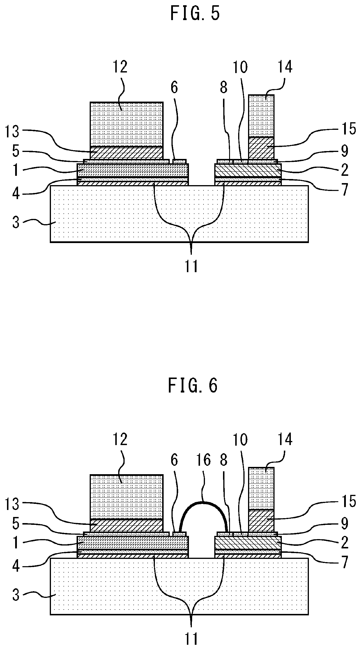
[0045]FIG. 13 is a cross-sectional view illustrating a semiconductor device according to a second embodiment. In the present embodiment, the wiring chip 2 and the connection member 16 are not provided, and the control electrode member 14 is bonded to the control electrode 6 of the semiconductor chip 1 via the second bonding material 15. Other configurations are similar to those in the first embodiment.
[0046]Subsequently, a manufacturing method of the semiconductor device according to the present embodiment will be described. FIGS. 14 to 16 are cross-sectional views illustrating the manufacturing method of the semiconductor device according to the second embodiment. First, as illustrated in FIG. 14, the semiconductor chip 1 is bonded to the substrate 3. Then, as illustrated in FIG. 15, the main electrode member 12 is bonded to the main electrode 5 via the first bonding material 13. The control electrode member 14 is bonded to the control electrode 6 via the second bonding material 15.
[0047]Then, as illustrated in FIG. 16, a semi-finished product including the semiconductor chip 1, the substrate 3, the main electrode member 12 and the control electrode member 14, which are bonded, is put into the mold 18. In this event, the buffer material 19 is provided between the main electrode member 12 and the mold 18 and between the control electrode member 14 and the mold 18. The semiconductor chip 1, the substrate 3, the main electrode member 12 and the control electrode member 14 are sealed with the sealing material 17 by injecting the sealing material 17 into the mold 18 in a state where the distal end surfaces of the main electrode member 12 and the control electrode member 14 are pressed against the buffer material 19.
[0048]The buffer material 19 is removed from the upper surface of the semiconductor device when the semiconductor device is removed from the mold 18 after sealing. Through the above-described process, the semiconductor device in which the distal end surfaces of the main electrode member 12 and the control electrode member 14 are exposed from the sealing material 17 is manufactured without grinding the sealing material 17. By this means, it is possible to reliably lead the electrode members out of the upper surface of the device while preventing increase in manufacturing cost in a similar manner to the first embodiment. In a case of a semiconductor device such as a semiconductor product having small capacity, which includes less semiconductor chips connected in parallel, there is a case where the present embodiment in which electrodes are individually led out of the semiconductor chip 1 and connected to an external circuit without using the wiring chip 2 is preferable because manufacturing cost can be reduced.
[0049]The semiconductor chip 1 is not limited to a chip formed of silicon, but instead may be formed of a wide-bandgap semiconductor having a bandgap wider than that of silicon. The wide-bandgap semiconductor is, for example, a silicon carbide, a gallium-nitride-based material, or diamond. A semiconductor chip formed of such a wide-bandgap semiconductor has a high voltage resistance and a high allowable current density, and thus can be miniaturized. The use of such a miniaturized semiconductor chip enables the miniaturization and high integration of the semiconductor device in which the semiconductor chip is incorporated. Further, since the semiconductor chip has a high heat resistance, a radiation fin of a heatsink can be miniaturized and a water-cooled part can be air-cooled, which leads to further miniaturization of the semiconductor device. Further, since the semiconductor chip has a low power loss and a high efficiency, a highly efficient semiconductor device can be achieved.
[0050]Obviously many modifications and variations of the present disclosure are possible in the light of the above teachings. It is therefore to be understood that within the scope of the appended claims the invention may be practiced otherwise than as specifically described.
[0051]The entire disclosure of Japanese Patent Application No. 2021-045845, filed on Mar. 19, 2021 including specification, claims, drawings and summary, on which the convention priority of the present application is based, is incorporated herein by reference in its entirety.

PUM

no PUM

Description & Claims & Application Information

We can also present the details of the Description, Claims and Application information to help users get a comprehensive understanding of the technical details of the patent, such as background art, summary of invention, brief description of drawings, description of embodiments, and other original content. On the other hand, users can also determine the specific scope of protection of the technology through the list of claims; as well as understand the changes in the life cycle of the technology with the presentation of the patent timeline. Login to view more.

Similar technology patents

Housing

ActiveUS20200388958A1prevent increase in cost
Owner:YAZAKI CORP

Substrate processing apparatus and method

InactiveUS20090156019A1prevent increase in coststably control temperature
Owner:TOKYO ELECTRON LTD

Optical disk apparatus and computer readable recording medium storing program

InactiveUS20050036767A1prevent increase in cost
Owner:YAMAHA CORP

Classification and recommendation of technical efficacy words

  • prevent increase in cost

Substrate processing apparatus and method

InactiveUS20090156019A1prevent increase in coststably control temperature
Owner:TOKYO ELECTRON LTD

Optical disk apparatus and computer readable recording medium storing program

InactiveUS20050036767A1prevent increase in cost
Owner:YAMAHA CORP

Housing

ActiveUS20200388958A1prevent increase in cost
Owner:YAZAKI CORP
Why Eureka
Try Eureka