Vertical field effect transistor and method for the formation thereof

Pending Publication Date: 2022-11-17
ROBERT BOSCH GMBH
View PDF0 Cites 0 Cited by
  • Summary
  • Abstract
  • Description
  • Claims
  • Application Information

AI Technical Summary

Benefits of technology

[0005]One object of the present invention is to provide a vertical field effect transistor and a method for th

Problems solved by technology

Such narrow semiconductor fins may no longer be able to be manufactured using conventional photolithography, as is typically used in the mass production of pow

Method used


Image

  • Vertical field effect transistor and method for the formation thereof
  • Vertical field effect transistor and method for the formation thereof
  • Vertical field effect transistor and method for the formation thereof

Examples


Example

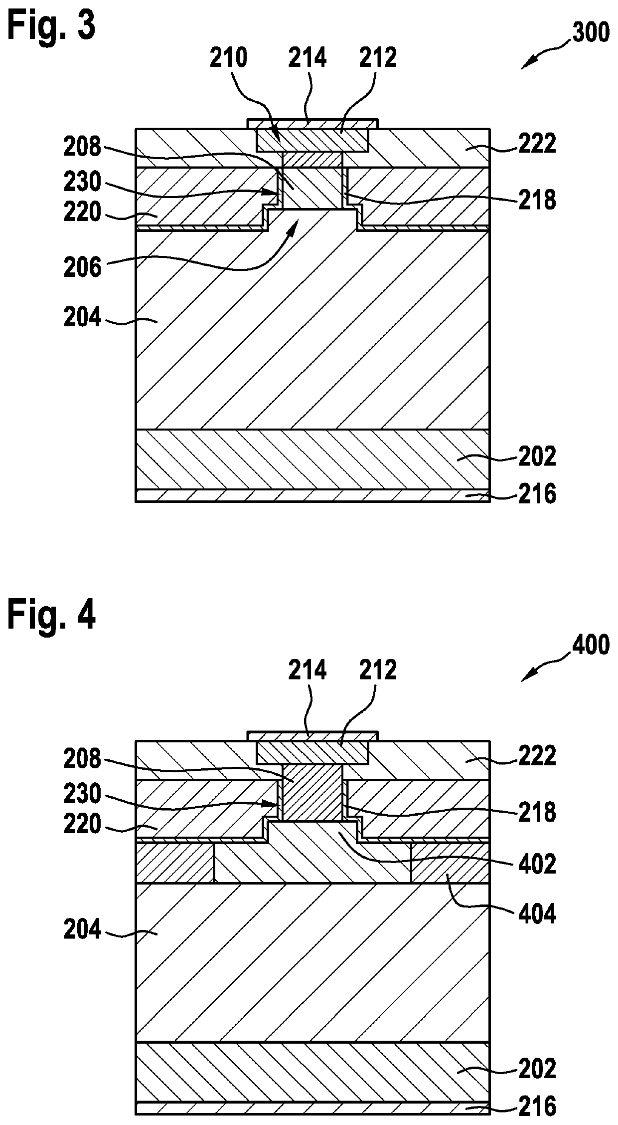
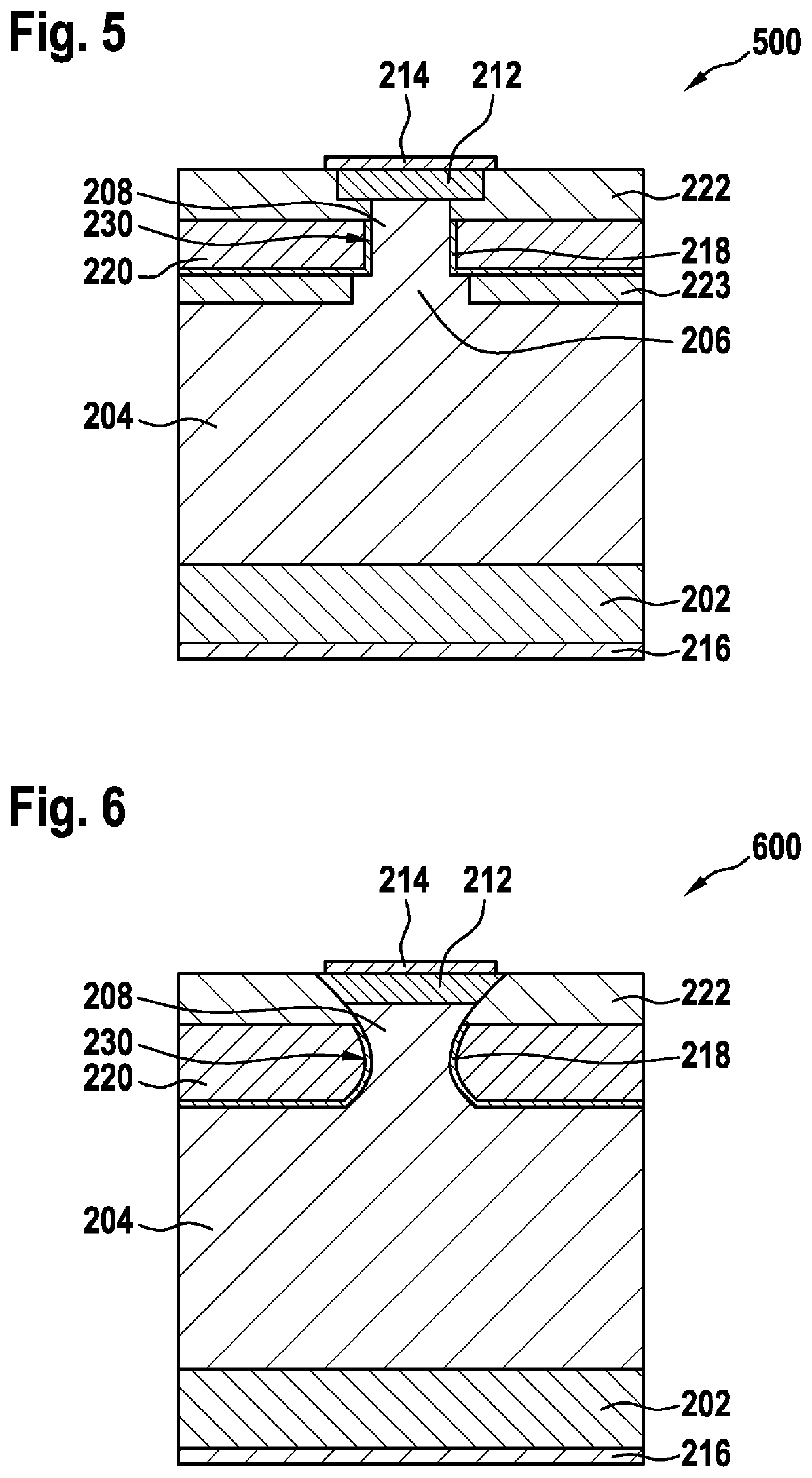
[0015]In the following detailed description, reference is made to the figures, which form a part of this description and in which specific exemplary embodiments are shown for illustration, in which the present invention may be implemented. It is obvious that other exemplary embodiments may be used and structural or logical modifications may be carried out without departing from the scope of protection of the present invention. The features of the various exemplary embodiments described herein may be combined with one another if not specifically indicated otherwise. The following detailed description is therefore not to be interpreted restrictively. In the figures, identical or similar elements are provided with identical reference numerals, if appropriate.

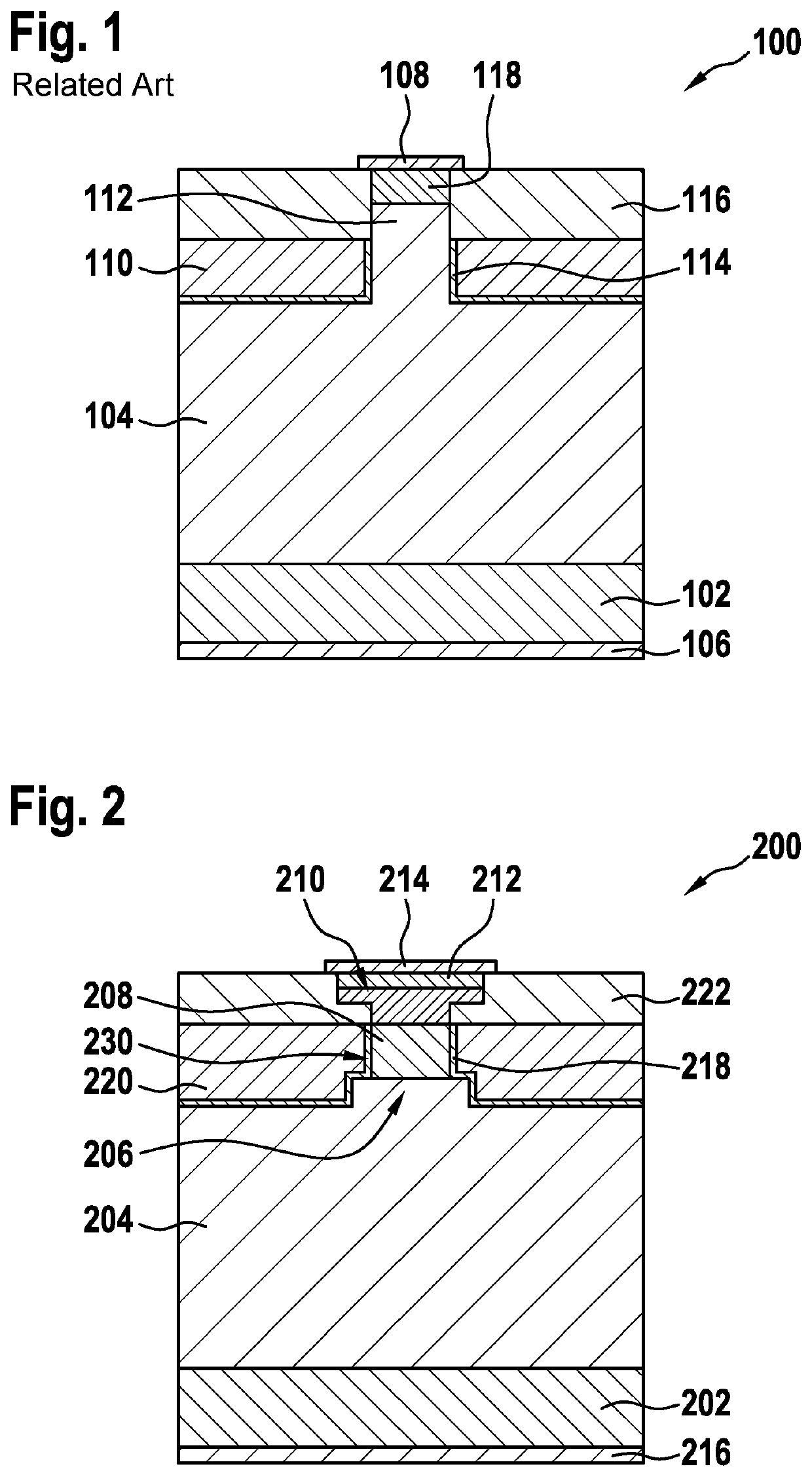
[0016]FIG. 2 shows a schematic sectional representation of a vertical field effect transistor 200 according to various specific embodiments. In various specific embodiments, vertical field effect transistor 200 includes a drift are...


PUM


Abstract

A vertical field effect transistor. The vertical field effect transistor includes: a drift area; a semiconductor fin on or above the drift area; a connection area on or above the semiconductor fin; and a gate electrode, which is formed adjacent to at least one side wall of the semiconductor fin, the semiconductor fin, in a first section, which is situated laterally adjacent to the gate electrode, having a lesser lateral extension than in a second section, which contacts the drift area, and/or than in a third section, which contacts the connection area.

Description

FIELD[0001]The present invention relates to a vertical field effect transistor and a method for the formation thereof.BACKGROUND INFORMATION[0002]In the automotive field, approaches for power semiconductors that switch rapidly and without loss are in demand with the progressing development toward electromobility. The simultaneous trend from lateral to vertical components and the trend of silicon technology, which has been established for decades, toward so-called “wide band gap” materials, i.e., semiconductor materials including a wide band gap, for example silicon carbide (SiC) or gallium nitride (GaN), has resulted here in the development of novel component concepts and manufacturing processes.[0003]For the application of semiconductors including a wide band gap, the use of so-called power FinFETs (Fin=fin, FET=field effect transistor) may be advantageous. In conventional MOSFETs or MISFETs, the actively switchable component is provided by an inversion channel—for example, by the ...

Claims


Application Information

Patent Timeline
IPC IPC(8): H01L29/78H01L29/16H01L29/20H01L29/06H01L29/66
CPCH01L29/7828H01L29/1608H01L29/2003H01L29/063H01L29/66068H01L29/66522H01L29/66666H01L29/0847H01L29/0619H01L29/0657
Inventor BARINGHAUS, JENSKREBS, DANIELSCHOLTEN, DICK
Owner ROBERT BOSCH GMBH
Why Eureka
Try Eureka