

Mosaic polishing pads and methods relating thereto
a technology of polishing pads and mosaics, applied in the field of polishing pads, can solve the problems of large unusable portions of material, large size of pads, and difficulty in manufacturing free polishing pads
- Summary
- Abstract
- Description
- Claims
- Application Information
AI Technical Summary
Benefits of technology
Problems solved by technology
Method used
Image

Examples
Embodiment Construction
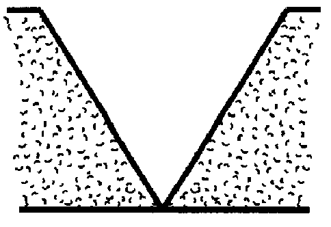
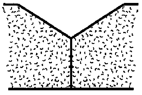
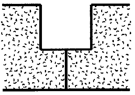
Thirty-six silicon 100P, acid wafers were polished using a mosaic pad. The periphery surface profile of the tiles was a straight line extending perpendicularly from the front surface to the back surface. Seams were not recessed. Pressure sensitive adhesive was used to mount the tiles to a PET sheet, and to mount the mosaic pad to a platen.
Pad characteristics were as follows:
Pad material: Suba 500, manufactured by Rodel, Inc. of Newark, Del.
Tile shape: hexagonal
Tile size: 12 inches as measured perpendicularly from side to opposite side
Total mosaic pad diameter: 36 inches
Polishing was performed on a Siltec 3800 polishing machine. The polishing parameters were as follows:
Time: 20 minutes
Down force: 5.5 psi at the wafer face
Platen speed: 60 rpm
Carrier speed: 60 rpm
Slurry flow: 250 ml / minute
Slurry type: Nalco 2350, a silica based slurry for stock polishing, diluted 20 parts DI H.sub.2 O to 1 part slurry.
For comparison, twenty-three wafers were polished using a 36 inch Suba 500 pad under ...
PUM
| Property | Measurement | Unit |
|---|---|---|
| angle | aaaaa | aaaaa |
| size | aaaaa | aaaaa |
| diameter | aaaaa | aaaaa |
Abstract
Description
Claims
Application Information