
Electrode plate, process for producing the plate, liquid crystal device including the plate and process for producing the device

Inactive Publication Date: 2000-02-08
CANON KK
View PDF13 Cites 9 Cited by
  • Summary
  • Abstract
  • Description
  • Claims
  • Application Information

AI Technical Summary

Benefits of technology

In the above embodiment (Second Embodiment), the color filter-forming step may be performed before the metal electrode-forming step.
Further, the metal electrodes 12 may be formed on the color filter 111 as in an electrode plate 110 as shown in FIG. 16.
Referring to FIG. 16, a color filter 111 is formed on the entire surface of the glass substrate 11. On the closer filter 111, the metal electrodes 12 ar formed so as to leave a spacing therebetween where respective color filter segments of R, G and B are disposed.
Specifically, as shown in FIG. 17A, the color filter-forming step is first performed to form the color filter 111 on the glass substrate 11 and thereon, the metal electrodes 12 are formed at a prescribed part of the color filter 111. Thereafter, a structure shown in FIG. 7B is formed through the resin-supplying step, the resin-molding step, the resin-curing step, and the peeling step. Then, the transparent electrodes 36 are formed on the above structure to prepare an electrode plate 110 as shown in FIG. 17C.
In this embodiment, the color filter layer 111 may be formed by various methods, including a photolithographic process, a printing process (wet-coating method), a sublimation transfer method, and an ink jet method. In the case of using the ink jet method, an ink-receptive (acceptable) layer is formed on the entire glass substrate 11 by wet-coating, such as spin coating. Thereafter, a prescribed ink including a dye may be injected into the ink-receptive layer with a high accuracy, thus impregnating the layer with the ink.
A third embodiment of the electrode plate according to the present invention will be explained with reference to FIG. 18 and FIGS. 19A-19C.

Problems solved by technology

However, these transparent electrodes 6 generally have a high resistivity, so that they have caused a problem of voltage waveform deformation due to electrical signal delay along with increases in resolution an size of the display area and in driving speed of the display device.
In order to solve the problem it may be possible to increase the thickness of the transparent electrodes 6, but the formation of such thick transparent electrodes requires increased time and cost and is liable to lower adhesiveness to the glass substrate 1.
As a result, an amount of light passing through the resultant liquid crystal display device is decreased, i.e., an opening rate of the display device is lowered, thus resulting in a dark image.
Further, the formation of the masking layer 21 leads to complicated production steps and increased production cost.
However, it has been difficult to find out such an ideal photosensitive resin satisfying the above requirements, thus failing to actually practice the above production process.
As a result, a transparent electrode 36 formed on the UV-cured resin layer (insulating layer) 33 is liable to lose its flatness, thus leading to an irregularity in threshold voltage and alignment defects in some cases.
On the other hand, if the inclination angle exceeds 60 degrees, the transparent electrode 36 is liable to cause a breakage thereof at the lateral end portion 33b (of the UV-cured resin layer 33), thus resulting in conduction failure.
Further, if the difference in height is above 5 .mu.m, it is difficult to partially cover the end portion of the metal electrode surface while retaining a prescribed inclination angle of the lateral end 33b, thus resulting in difficulties as in the case of the inclination angle of below 15 degrees.
Above 5000 .ANG., a light transmittance of the resultant transparent electrodes is liable to be lowered, thus resulting in a deterioration in display quality when used in a display device.

Method used


Image

  • Electrode plate, process for producing the plate, liquid crystal device including the plate and process for producing the device
  • Electrode plate, process for producing the plate, liquid crystal device including the plate and process for producing the device
  • Electrode plate, process for producing the plate, liquid crystal device including the plate and process for producing the device

Examples


first embodiment

The resultant liquid crystal device provided advantageous effects similar to those in First Embodiment described hereinabove.

example 2

A liquid crystal device was prepared in the same manner as in Example 1 except that in the resin-supplying step a UV-curable resin 33L was placed dropwise on a metal wiring plate A1, whereby good results were attained similarly as in Example 1.

example 3

A color liquid crystal device was prepared in the same manner as in Example 1 except that a 1 .mu.m-thick color filter layer 101 comprising segments of red (R), green (G) and blue (B) as shown in FIG. 14 was formed in the same manner as in Second Embodiment described above and an additional UV-ray irradiation was performed.

More specifically, the color filter layer 101 was formed with pigment-type color filter materials (mfd. by Ube Kosan K. K.) by a photolithographic process including an etching step.

The irradiation of UV-rays was performed for 2 min. from the UV-curable resin side after the peeling step.

The resultant color liquid crystal device provided good color images and good results similarly as in Example 1.


PUM


Abstract

An electrode plate for a liquid crystal device is constituted by a light-transmissive substrate, a plurality of metal electrodes disposed on the light-transmissive substrate with a spacing therebetween, an insulating layer disposed at the spacing, and a plurality of transparent electrodes disposed on the insulating layer and each electrically connected with an associated metal electrode at a first end portion thereof. The first end portion of the transparent electrode is located closer to the light-transmissive substrate than an adjacent end portion of an adjacent transparent electrode. The electrode plate is effective in providing a liquid crystal device with a wider optical modulation region while improving image qualities.

Description

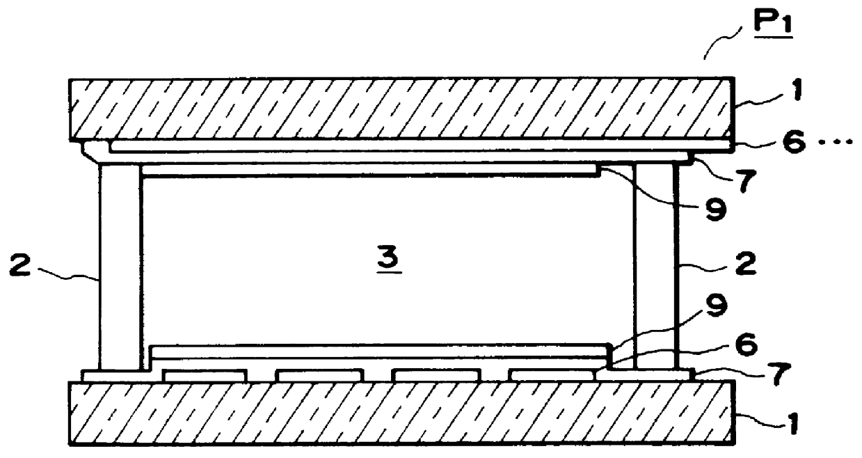
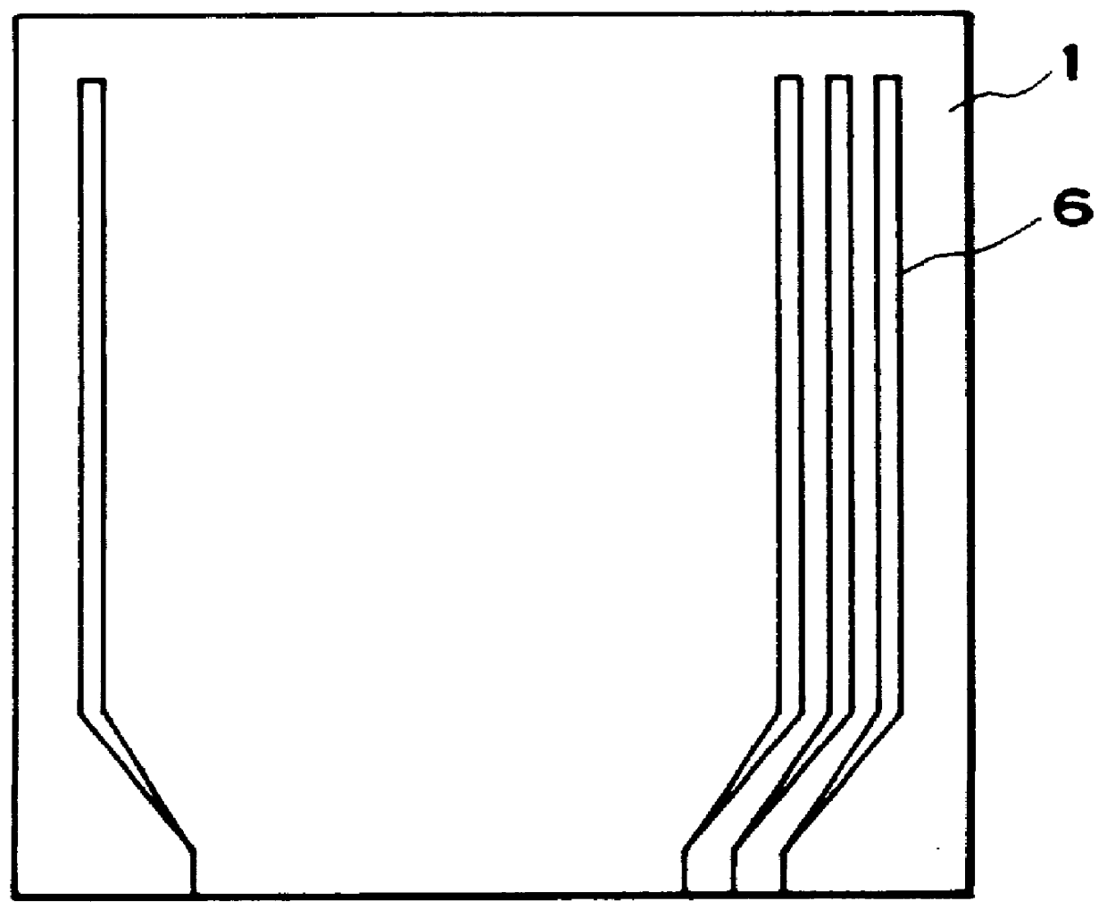
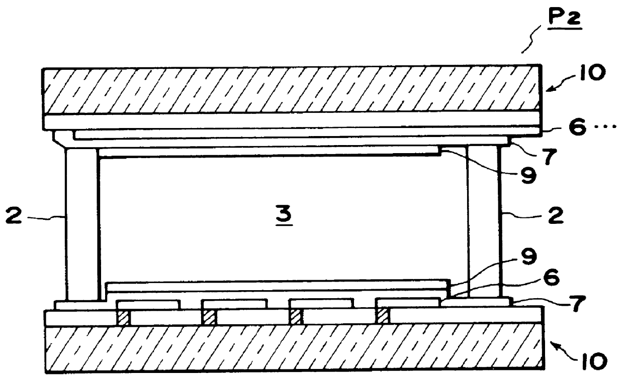
FIELD OF THE INVENTION AND RELATED ARTThe present invention relates to an electrode plate, particularly an electrode plate provided with metal electrodes formed along transparent electrodes, and a production process and apparatus of the electrode plate. The present invention also relates to a liquid crystal device including the electrode plate and a production process thereof.Liquid crystal display devices (cells) using a liquid crystal for displaying information have been used in various fields.The cell structure of the liquid crystal devices has also been modified with increases in resolution and size required in recent years as follows.(1) FIGS. 1A and 1B are schematic sectional and plan views, respectively, illustrating a liquid crystal display device of an initial stage.Referring to FIG. 1A, a liquid crystal display device P1 includes a pair of glass substrates 1 oppositely disposed in substantially parallel with each other. Each glass substrate 1 is coated with a plurality of ...

Claims


Application Information

Patent Timeline
IPC IPC(8): G02F1/13G02F1/1343G02F1/1333G02F1/1345
CPCG02F1/134336G02F1/133345
Inventor TOMONO, HARUOKAMIO, MASARUTOKUNAGA, HIROYUKIMATSUO, YUJI
Owner CANON KK
Learn More