Check patentability & draft patents in minutes with Patsnap Eureka AI!

ESD protection circuits

a protection circuit and metal oxide technology, applied in the direction of emergency protective arrangements for limiting excess voltage/current, pulse manipulation, pulse technique, etc., can solve the problems of esd stress, chip failure, electrostatic discharge,

Inactive Publication Date: 2000-02-15
STMICROELECTRONICS SRL
View PDF7 Cites 38 Cited by
  • Summary
  • Abstract
  • Description
  • Claims
  • Application Information

AI Technical Summary

Problems solved by technology

Electrostatic discharge (ESD) is one of the most prevalent causes for chip failures in both chip manufacturing and field operations.
In addition to human handling, contact with machines can also cause ESD stress.
Since body resistance is absent, the stress can be even more severe and with higher current levels.
Small chip size, small diameter power bussing metal runs, and limited power / ground pins present particular problems with ESD irrespective of the type of CMOS device.
Larger chips have more capacitance (more available for charge storage) and are easier to handle; the smaller the chip, the more difficult the ESD problem.
Moreover, narrow power bussing metal runs means the current carrying capacity of the metal is limited (acts like a fuse) and ofttimes, a static discharge will blow (melt to short or open) the line.
In the same manner limited ground line area is an obvious problem, because the line cannot dissipate heat due to excess current fast enough and sometimes causes adjacent device breakdown.

Method used


Image

  • ESD protection circuits
  • ESD protection circuits
  • ESD protection circuits

Examples


Embodiment Construction

)

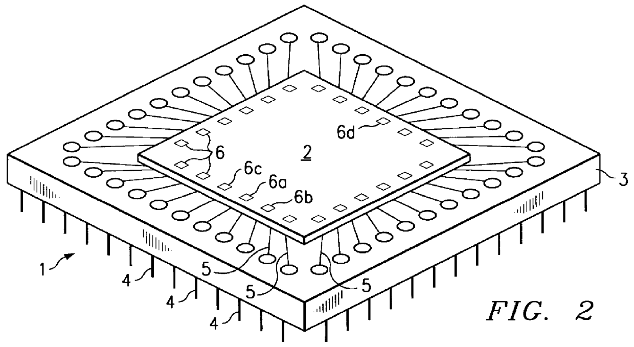
Turning now to the drawings, and specifically FIG. 2 thereof, an exemplary integrated circuit (IC) package 1 is illustrated as including an integrated circuit MOS device 2 thereon including ESD protection means constructed in accordance with the present invention. The package 1 includes an insulating platform 3 from which pins 4 depend from the lower surface thereof. The pins 4 pass through the platform and connect to leads 5, which connect in turn to input / output pads 6 on the MOS IC chip 2. While certain of the protection means may be incorporated externally of the chip 2 on the insulating platform 3, as shall be illustrated hereinafter, the ESD protection means is preferably located in the device 2 so that protection will include the handling of the device for securing it to the platform 3 of the package 1. In this connection, the present invention is not meant to exclude other ESD protection which may be imposed by the packaging of the integrated circuit 2.

Prior to discussing t...


PUM


Abstract

Electro-static-discharge (ESD) protection circuits are supplied for inhibiting the destruction of buffers, drivers, logic and memory cells in Metal-Oxide-Semiconductor (MOS) devices such as a CMOS device including Static-Random-Access-Memory (SRAM). This is accomplished by tiering diodes adjacent the input of the chip and in certain specific areas internally of the chip (e.g. power supplies etc.) providing bidirectional diode protection from over-voltage.

Description

1. Field of the InventionThe present invention relates to protection for Metal Oxide Semiconductor (MOS) integrated circuits such as Static-Random-Access-Memory (SCRAM) and more particularly relates to protection schemes against electrostatic discharge from either human or machine handling, while minimizing effects on the circuits to which the schemes are applied.2. Description of Related ArtElectrostatic discharge (ESD) is one of the most prevalent causes for chip failures in both chip manufacturing and field operations. ESD can occur when the charges stored in machines or the human body are discharged to the chip on contact or by static induction. FIG. 1 shows different models for ESD testing. FIG. 1A shows the test for duplicating the human body model (HBM); FIG. 1B the test for duplicating the machine model (MM), and; FIG. 1C the test for duplicating the Charged Device Model (CDM).A human walking across synthetic carpet in 80% relative humidity can potentially induce 1.5 kV of s...

Claims


Application Information

Patent Timeline
IPC IPC(8): H01L27/02
CPCH01L27/0251H01L27/0255H01L27/0266
Inventor SO, JASON SIUCHEONG
Owner STMICROELECTRONICS SRL
Features
  • R&D
  • Intellectual Property
  • Life Sciences
  • Materials
  • Tech Scout
  • Unparalleled Data Quality
  • Higher Quality Content
  • 60% Fewer Hallucinations
Learn More