Semiconductor type yaw rate sensor

a sensor and yaw rate technology, applied in the field of yaw rate sensors of semiconductor type, can solve problems such as the complexity of the structure of the yaw rate sensor

Inactive Publication Date: 2000-02-22
DENSO CORP
View PDF19 Cites 70 Cited by
  • Summary
  • Abstract
  • Description
  • Claims
  • Application Information

AI Technical Summary

Problems solved by technology

Therefore, the structure of the ya

Method used


Image

  • Semiconductor type yaw rate sensor
  • Semiconductor type yaw rate sensor
  • Semiconductor type yaw rate sensor

Examples


first embodiment

(First Embodiment)

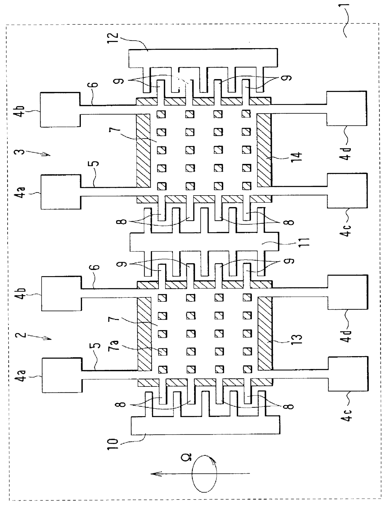
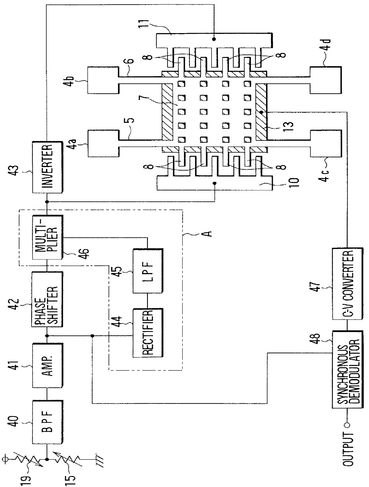
As shown in FIG. 1, a semiconductor type yaw rate sensor has beam structures (movable structures) 2, 3 on an upper surface of a semiconductor substrate 1. The beam structures 2, 3 are caused to vibrate in opposite phase, and an output signal from each of the beam structures 2, 3 is generated. A yaw rate is detected due to differential detection of the output signals from the beam structures 2, 3.

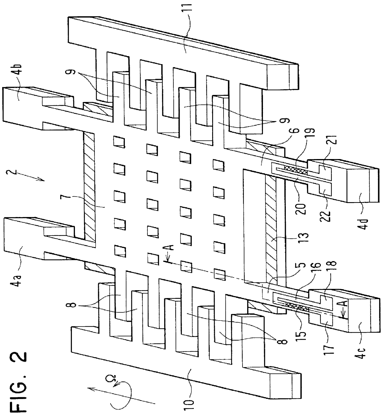
The beam structure 2 includes four anchor portions 4a, 4b, 4c and 4d disposed on the substrate 1 with predetermined gaps therebetween. A beam portion 5 is installed between the anchor portions 4a, 4c and a beam portion 6 is installed between the anchor portions 4b, 4d. A weighted portion (mass portion) 7a is provided between the beam portions 5, 6. Therefore, the beam portions 5, 6 are connected via the weighted portion 7.

In the weighted portion 7, plural holes 7a that vertically penetrate the weighted portion 7 are formed. Also, plural movable electrodes 8 for vibration us...


PUM


Abstract

A semiconductor type yaw rate sensor has a substrate, a beam structure formed from a semiconductor material and having at least one anchor portion disposed on the substrate, a weighted portion located above the substrate a predetermined gap therefrom, and a beam portion which extends from the anchor portion and supports the weighted portion. A movable electrode is formed onto the weighted portion, and a fixed electrode is formed on the substrate in such a manner that the fixed electrode faces the movable electrode. When a drive voltage is applied between the movable electrode and the fixed electrode, the beam structure is forcibly caused to vibrate in a direction that is horizontal relative to a substrate surface plane. In this yaw rate sensor, a strain gauge to monitor forced vibration of the beam structure is formed in the beam portion. As a result, the forced vibration of the beam structure can be monitored with a simple structure.

Description

1. Field of the InventionThe present invention relates to a semiconductor type yaw rate sensor having a beam structure formed from a semiconductor material.2. Related ArtA conventional semiconductor type yaw rate sensor is disclosed in JP-A-H.8-148698. In this semiconductor type yaw rate sensor, a beam structure is formed from a semiconductor material and is located a predetermined distance above an upper surface of a substrate. The beam structure is forcibly caused to vibrate in a horizontal direction relative to the substrate surface plane. A yaw rate is detected based on vertical displacement of the beam structure relative to the substrate surface plane.In this semicondutor type yaw rate sensor, to detect vibrating state of the beam structure in the horizontal direction, a movable gate electrode is provided in the beam structure, and source and drain electrodes are formed in the substrate. Due to this arrangement, the vibrating state of the beam structure in the horizontal direct...

Claims


Application Information

Patent Timeline
IPC IPC(8): G01C19/56G01P15/08G01L1/18G01C19/5719G01P15/00G01P15/12G01P15/14H01L29/84
CPCG01C19/5719G01P15/0802Y10S73/01G01P2015/0814
Inventor KANO, KAZUHIKOFUJITA, MAKIKOOHTSUKA, YOSHINORI
Owner DENSO CORP
Why Eureka
Try Eureka