Method of producing semiconductor devices and method of evaluating the same

a technology of semiconductor devices and semiconductor oxide films, which is applied in the direction of semiconductor/solid-state device testing/measurement, instruments, testing vessel construction, etc., can solve the problems of difficult to distinguish the effects of shapes, difficult to use data obtained from mos capacitors as data for gate oxide films, and often undergo insulation breakdown, etc., to achieve efficient evaluation of reliability

Inactive Publication Date: 2000-02-29
FUJITSU LTD
View PDF6 Cites 8 Cited by
  • Summary
  • Abstract
  • Description
  • Claims
  • Application Information

AI Technical Summary

Benefits of technology

is to provide a simulation method capable of efficiently evaluating the reliability of gate oxide films formed on elements, within short periods of time, to evaluate characteristics of a semiconductor device made up of elements of any size and any number, by improving the above-mentioned defects inherent in the prior art.

Problems solved by technology

The gate oxide film, however, often undergoes insulation breakdown due to defects in the steps of production, erroneous designing or conditions in which it is used, and it is becoming important to enhance the reliability of the gate oxide film, the properties of the gate oxide film and the life thereof.
It is not therefore possible to use the data obtained from the MOS capacitor as data for the gate oxide film.
(4) Reliability of the gate oxide film is affected depending upon its shape, but it is difficult to verify the effects of the shapes in a distinct manner.
So far, therefore, a considerable period of time was required for evaluating the reliability of the gate oxide film that is a basis for evaluating the characteristics of the semiconductor device, i.e., for evaluating characteristics, performance, shape, etc. of the transistor.
Besides, it is difficult to evaluate the desired gate oxide film from the obtained data.
Moreover, even when the gate oxide film was evaluated, the data were not adapted to evaluating the gate having a different form.

Method used


Image

  • Method of producing semiconductor devices and method of evaluating the same
  • Method of producing semiconductor devices and method of evaluating the same
  • Method of producing semiconductor devices and method of evaluating the same

Examples


second embodiment

the present invention will be explained hereunder.

As shown in the Table 1, three different conditions used in the process for making oxide films, were selected and three different kinds of semiconductor devices were produced.

Thereafter, the reliability of these oxide films were checked in accordance with the evaluation method as defined by the present invention.

The results thus obtained are indicated in Table 1.

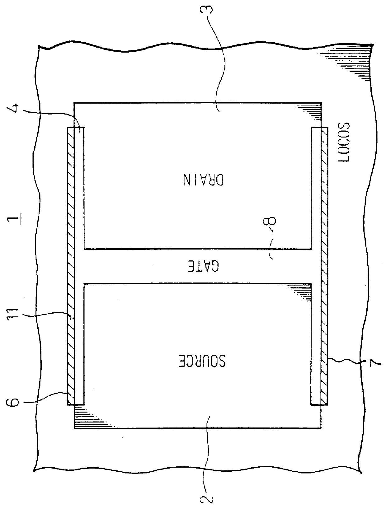
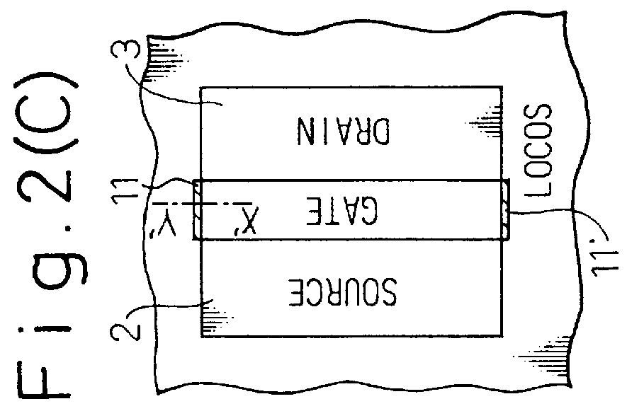
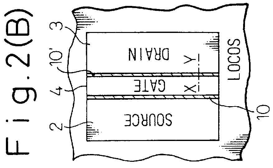
The three samples of the semiconductor devices No. 1 to No. 3 are formed each one of the evaluation gate patterns as shown in FIG. 4, utilizing each of the process conditions as indicated in Table 1, respectively.

Then, the value of QBD of each oxide film of the respective samples No. 1 to No. 3 were measured to thereby calculate each of the coefficients A1, A2 . . . B2, B3, and C for each one of the samples No. 1 to No. 3.

Thereafter, a value of the QBD of an integrated transistor circuit device, each one of the transistors having a width W=10 .mu.m and a length L=0.35 .mu.m, ...


PUM


Abstract

A simulation method capable of efficiently evaluating reliability of gate oxide films formed on the elements within short periods of time to evaluate characteristics of a semiconductor device made up of elements of any size and any number. In a semiconductor device having transistors formed thereon, a pattern for evaluating characteristics of a semiconductor device characterized in that gate area portions, gate bird's-beak portions and LOCOS bird's-beak portions, are factors affecting the insulation breakdown of the gate oxide film, are rendered to be variable, so that the shapes of these portions can be handled as independent parameters.

Description

1. Field of the InventionThe present invention relates to a method of evaluating semiconductor devices, a method of designing semiconductor devices and a method of producing the semiconductor devices. More specifically, the invention relates to a method of evaluation for producing semiconductor devices made up of the transistors that exhibit highly reliable characteristics and a method of producing semiconductor devices.2. Description of the Related ArtAmong transistors, an MOS transistor using a gate oxide film has heretofore been widely used. Accompanying the demand for fabricating MOS transistors in reduced sizes yet having improved performance, is a demand to form the gate oxide film with a reduced area and a reduced thickness.The gate oxide film, however, often undergoes insulation breakdown due to defects in the steps of production, erroneous designing or conditions in which it is used, and it is becoming important to enhance the reliability of the gate oxide film, the propert...

Claims


Application Information

Patent Timeline
Patent Type & Authority Patents(United States)
IPC IPC(8): H01L23/544G01R31/12G01R31/16G01R31/26H01L21/316H01L21/76
CPCH01L22/34H01L2924/0002H01L2924/00
Inventor HAMADA, MAKOTOSHONO, KEN
Owner FUJITSU LTD
Why Eureka
Try Eureka