
Square-law clamping circuit

Inactive Publication Date: 2000-02-29
MOTOROLA INC
View PDF13 Cites 11 Cited by
  • Summary
  • Abstract
  • Description
  • Claims
  • Application Information

AI Technical Summary

Problems solved by technology

This increased rate of current change causes a voltage drop across the inductance.
This can create a problem of having the internal supply at a different voltage than the voltage of the external supply.
This problem can cause the internal supply voltages to differ by so much from their external levels that signals input to the chip are recognized incorrectly.
However, the use of bipolar transistors creates additional problems.
One problem is that the increased rate of switching of output buffers with bipolar transistors has worsened the di / dt problem.
A second problem results from the fact that bipolar transistors degrade in the reverse biased condition and as reverse bias increases, the amount of degradation increases.
Therefore using bipolar transistors with a large reverse bias is subject to reliability problems in that the transistors may degrade over time, ultimately resulting in a failure of the entire integrated circuit.
A third problem arises from the nature of a bipolar transistor itself.
For some circuit applications, such as output buffers, the possibility that the output voltage will self-boost beyond the desired value is harmful to operation of the circuit.
A fourth problem is that output buffers must be able to operate well under a variety of load conditions.

Method used


Image

  • Square-law clamping circuit
  • Square-law clamping circuit
  • Square-law clamping circuit

Examples


Embodiment Construction

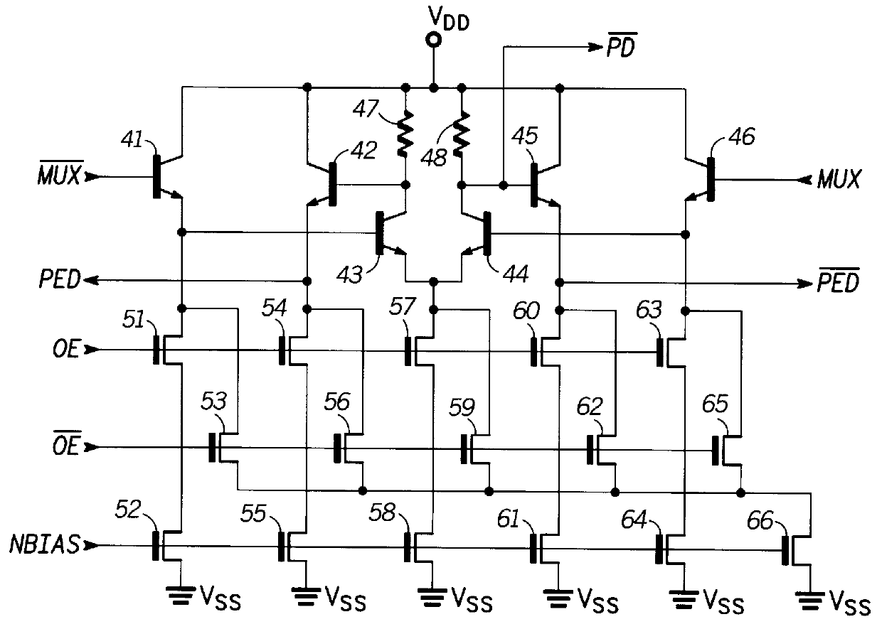
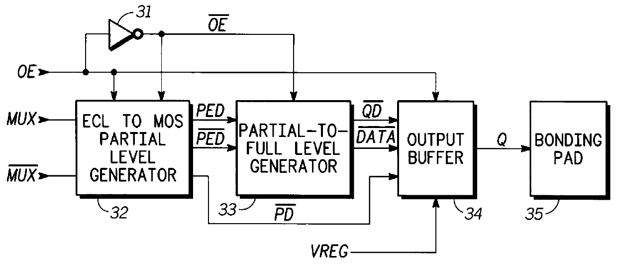
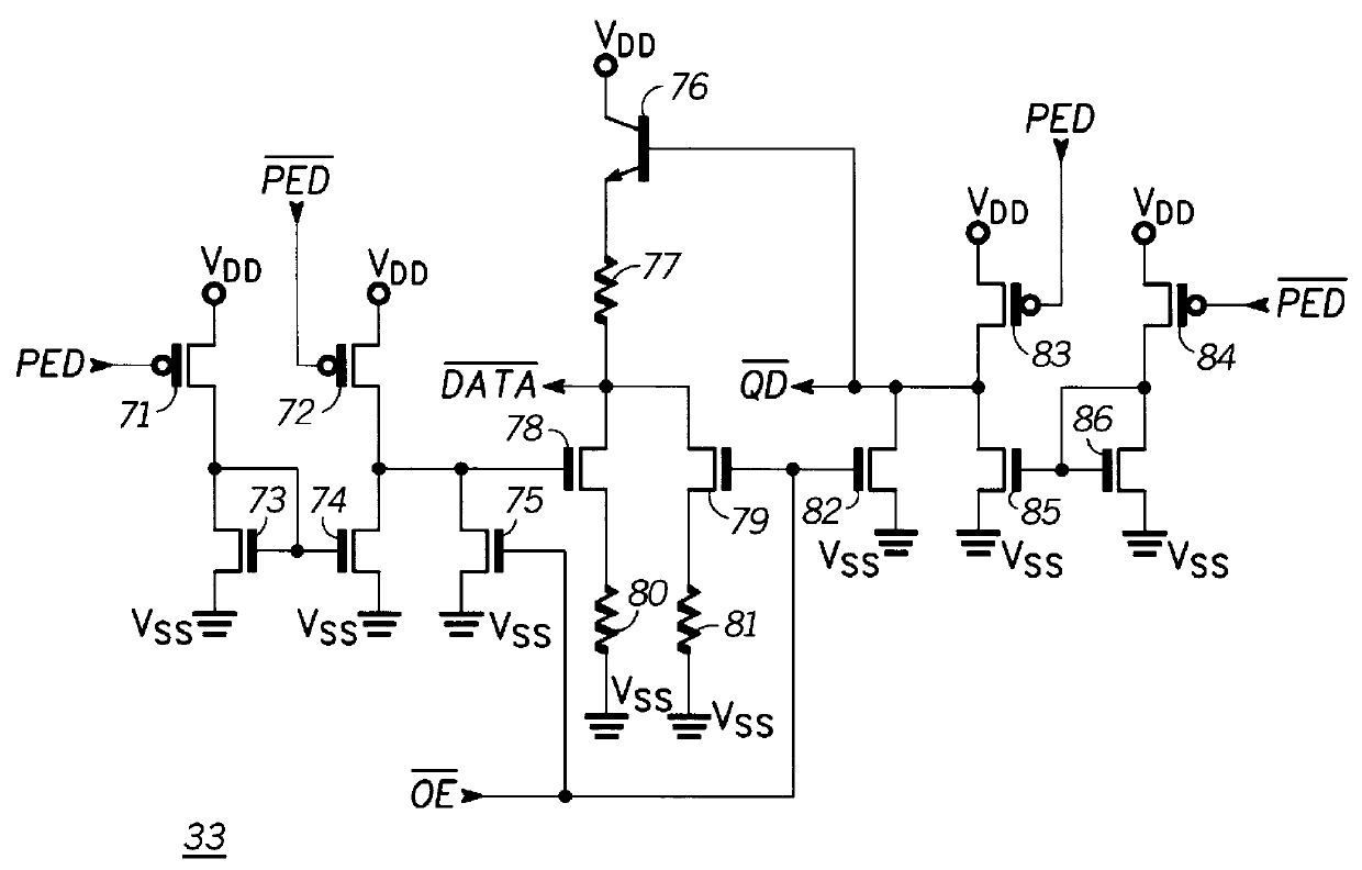
FIG. 1 illustrates in block form a portion of an integrated circuit 30 including an output buffer 34 in accordance with the present invention. Portion 30 includes an inverter 31, an ECL-to-MOS partial level generator 32, a partial-to-full level generator 33, output buffer 34, and a bonding pad 35. The function of each of the blocks of portion 30 will be more clearly understood in connection with the following description with regard to FIGS. 2-6. However, FIG. 1 is helpful in understand the overall operation of output buffer 34.

A signal labelled "Q" is provided by output buffer 34 in response to an output enable signal, labelled "OE". Signal OE is provided to generator 32 and output buffer 34. However for more convenient use inverter 31 inverts signal OE to provide its complement, labelled "OE", which is provided to generator 32 and generator 33. Generator 32 receives a digital signal represented as a differential voltage between signals labelled "MUX" and "MUX". In the illustrated ...


PUM


Abstract

A square-law clamping circuit (99, 120) sinks a current from an input / output terminal proportional to a square of a difference between a voltage thereon and a reference voltage. A first MOS transistor (130) has a source for receiving the reference voltage, a gate, and a drain coupled to its gate. A current source (134) coupled to the drain of the first MOS transistor (130) sources a predetermined current therefrom. A second MOS transistor (132) has a source providing the input / output terminal (100, 121), a gate coupled to the drain of the first MOS transistor (130), and a drain. A current sink (135) coupled to the drain of the second MOS transistor (132) sinks a current therefrom.

Description

FIELD OF THE INVENTIONThis invention relates generally to electrical circuits, and more particularly, to clamping circuits.BACKGROUND OF THE INVENTIONIn integrated circuits, there is generally a piece of silicon known as a die or chip which contains electrical circuits. The chip has bonding pads which are used as interconnection points to other circuitry. For example, the chip may be connected to a lead frame by tiny wires. The lead frame in turn has leads which are used for connecting to a printed circuit board as part of a larger system. The leads of the lead frame have a certain amount of inductance as well as capacitance and resistance. There is also some inductance in the wire connecting the bonding pad to the lead frame. The wire inductance, however, is significantly less than that of the lead frame. The connection of a lead of the lead frame to a circuit board also adds some inductance. As the switching speeds of integrated circuits have increased, this cumulative inductance ...

Claims


Application Information

Patent Timeline
IPC IPC(8): G06F7/552G06F7/48G06F7/556
CPCG06F7/552G06F7/556H03K5/08
Inventor FLANNAGAN, STEPHEN
Owner MOTOROLA INC
Learn More