Vertically stacked field programmable nonvolatile memory and method of fabrication

a nonvolatile memory and vertical stack technology, applied in the field of low cost, high density semiconductor memories, can solve the problems of high cost, flexibility has a cost, and the mask rom is not erasable, and achieves the effect of increasing the price per bit, increasing the cost, and increasing the cos

Inactive Publication Date: 2000-03-07
RHOMBUS
View PDF42 Cites 2094 Cited by
  • Summary
  • Abstract
  • Description
  • Claims
  • Application Information

AI Technical Summary

Problems solved by technology

In contrast, the contents of mask ROMs are permanently stored during manufacture, therefore mask ROMs are not erasable and are effectively "write only once, at the factory" memories.
But this flexibility has a cost: field programmable memories generally achieve lower densities (fewer bits per chip) and higher cost (larger price per bit) than mask ROMs.
Unfortunately, such a device has yet not been available.
First, since mask ROMs do not support erase or rewrite functions, their peripheral circuits need not contain any dedicated circuitry or I/O terminals for input-data steering, for write timing, or f

Method used


Image

  • Vertically stacked field programmable nonvolatile memory and method of fabrication
  • Vertically stacked field programmable nonvolatile memory and method of fabrication
  • Vertically stacked field programmable nonvolatile memory and method of fabrication

Examples


Embodiment Construction

A field programmable nonvolatile memory cell and memory array is disclosed. In the following description numerous specific details are set forth in order to provide a thorough understanding of the present invention. However, it will be apparent to one skilled in the art that the present invention may be practiced without these specific details. In other instances, well-known circuits and processes have not been described in detail in order not to obscure the present invention.

Overview of the Present Invention

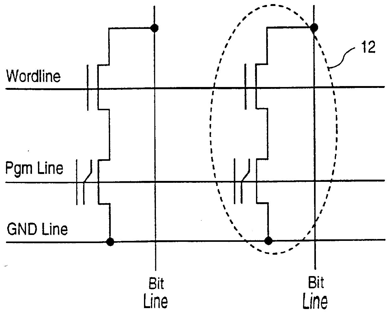
The field programmable nonvolatile memory cell of the present invention is built above, rather than in, a planar substrate. Therefore, this memory cell can be stacked vertically in numerous layers to form a three dimensional array. Each layer of memory cells interacts only with the layer above and the layer below, which makes vertical stacking of layers quite simple.

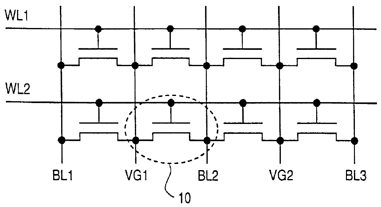
A unique organization of these cells in a three dimensional memory array disposed above a substrate, with peripher...


PUM


Abstract

A very high density field programmable memory is disclosed. An array is formed vertically above a substrate using several layers, each layer of which includes vertically fabricated memory cells. The cell in an N level array may be formed with N+1 masking steps plus masking steps needed for contacts. Maximum use of self alignment techniques minimizes photolithographic limitations. In one embodiment the peripheral circuits are formed in a silicon substrate and an N level array is fabricated above the substrate.

Description

1. Field of the InventionThis invention relates to low cost, high density semiconductor memories and, in particular, to semiconductor memories whose contents are "nonvolatile": data stored in the memory is not lost or altered when electrical power is removed.2. Background of the InventionThere is an ever-increasing demand for ever-denser semiconductor memories, and customers continue to purchase these memories in ever-greater quantities, even as the number of bits per chip quadruples (approximately) every three years. Increasingly higher densities are required, at ever lower costs, to meet the needs of the marketplace.Semiconductor nonvolatile memories may be divided into two categories: (1) those in which data is permanently written during the manufacturing process and whose contents cannot be subsequently changed, called "mask ROMs" or "factory programmed ROMs"; (2) those in which data may be supplied after the finished memory device leaves the factory. This latter category is cal...

Claims


Application Information

Patent Timeline
IPC IPC(8): G11C11/56G11C17/14G11C17/16H01L27/102H01L27/10
CPCG11C11/5692G11C13/003G11C17/16H01L27/1021G11C11/5678G11C2213/71G11C2213/76G11C17/10
Inventor JOHNSON, MARK G.LEE, THOMAS H.SUBRAMANIAN, VIVEKFARMWALD, PAUL MICHAELCLEEVES, JAMES M.
Owner RHOMBUS
Why Eureka
Try Eureka