Burn-in stress test mode

Inactive Publication Date: 2000-03-14
MICRON TECH INC
View PDF4 Cites 35 Cited by
  • Summary
  • Abstract
  • Description
  • Claims
  • Application Information

AI Technical Summary

Problems solved by technology

While this time-out feature conserves power and thus makes the device a low power device, devices having this time-out feature are difficult to stress test in a burn-in oven since

Method used


Image

  • Burn-in stress test mode
  • Burn-in stress test mode

Examples


Embodiment Construction

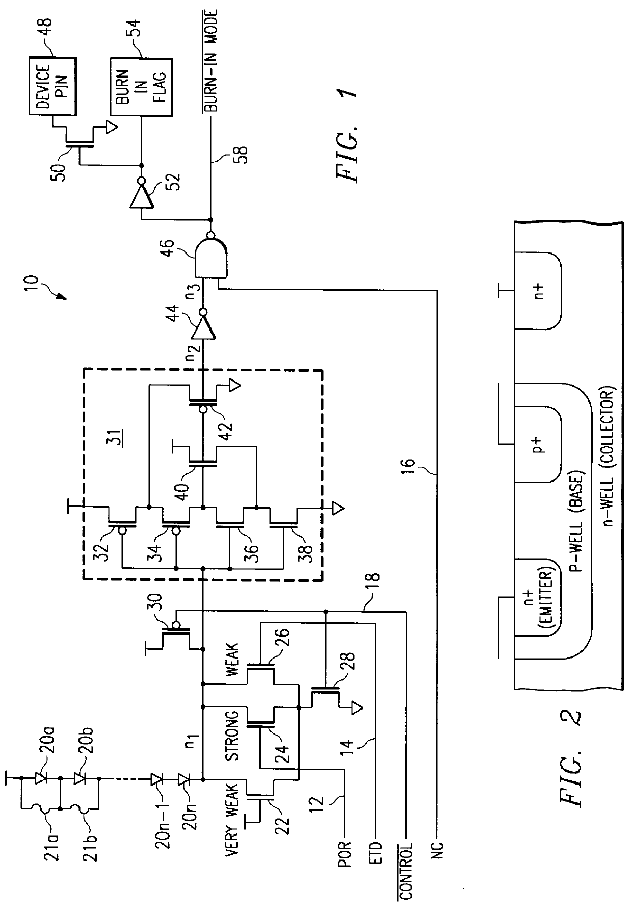
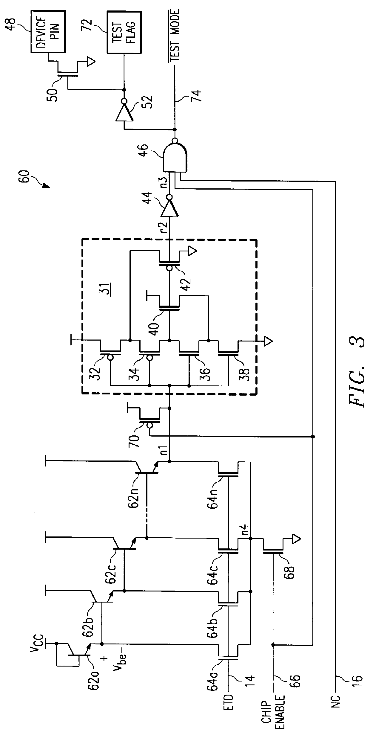
The present invention provides a burn-in stress test mode that is capable of disabling a time-out feature of an IC memory device during a stress test mode of the device in order to facilitate stress testing of the device in a burn-in oven in a timely and economical manner. The time-out feature of an IC memory device is disabled during the burn-in stress test mode by leaving on the wordlines of the device for the duration of the memory cycle for maximum burn-in efficiency.

A major concern of the present invention is the ability to enter into the burn-in stress test mode at the package level of the device. In many IC memory devices there may be no pins available which may be dedicated to enable or enter the burn-in stress test mode. On an asynchronous memory device, for instance, any pin sequence or combination of pin sequences may be needed for device operation and thus the use of device pins to enter the burn-in stress test mode is not a feasible solution. In addition to the dearth o...


PUM


Abstract

An integrated circuit structure and method provides a burn-in stress test mode that facilitates stress testing of an integrated circuit device in a burn-in oven. The integrated circuit structure and method is capable of disabling a time-out feature of an IC memory device during a stress test mode of the device in order to facilitate stress testing of the device in a burn-in oven. The integrated circuit structure provides for entry into the burn-in stress test mode when a supply voltage supplied to the integrated circuit device exceeds a predetermined voltage level and/or the temperature of the integrated circuit device exceeds a predetermined temperature level.

Description

1. Technical FieldThe present invention relates generally to Integrated Circuit (IC) memory devices and more specifically to burn-in stress testing of synchronous IC memory devices.2. Discussion of the Prior ArtLow power integrated circuit (IC) memory devices possess a time-out feature that enables the device to conserve power. The time-out feature of a static random access memory (SRAM) device, for instance, may conserve power by turning off all wordlines of a memory cell after a given period of time. For a 1 Meg SRAM device the time-out feature may cause the wordlines of the memory cell to be turned off after approximately 40 nS to 50 nS.While this time-out feature conserves power and thus makes the device a low power device, devices having this time-out feature are difficult to stress test in a burn-in oven since the wordlines must be on in order to stress the memory cells of the device. The devices cycle at no faster than several microseconds. Thus, for the majority of the time ...

Claims


Application Information

Patent Timeline
IPC IPC(8): G01R31/28G11C11/413G01R31/26G11C29/06
CPCG01R31/2856G01R31/287G01R31/2884
Inventor MCCLURE, DAVID CHARLES
Owner MICRON TECH INC
Why Eureka
Try Eureka