Clock distribution circuit in a semiconductor integrated circuit

a technology of integrated circuits and clocks, applied in the direction of generating/distributing signals, pulse techniques, instruments, etc., can solve the problems of erroneous circuit operation, clock skew, timing discrepancies,

Inactive Publication Date: 2000-03-14
FUJITSU LTD
View PDF5 Cites 30 Cited by
  • Summary
  • Abstract
  • Description
  • Claims
  • Application Information

AI Technical Summary

Problems solved by technology

If there are differences in length among wiring patterns from the origin of distribution of the clock signal to destinations to which the distributed clock signal is supplied, discrepancies arise in timing at which the clock signals arrive at the destinations (i.e., clock skew arises).
If clock skew occurs, there arises a risk that the flip-flop or the like takes in an erroneous signal or that unwanted whisker-like pulses are generated at an output of a logic gate, both resulting in erroneous operation of the circuit.
Further, in a case where a narrow wiring pattern is formed from copper in the same manner as is the aluminum wiring pattern, the...

Method used


Image

  • Clock distribution circuit in a semiconductor integrated circuit
  • Clock distribution circuit in a semiconductor integrated circuit
  • Clock distribution circuit in a semiconductor integrated circuit

Examples


first embodiment

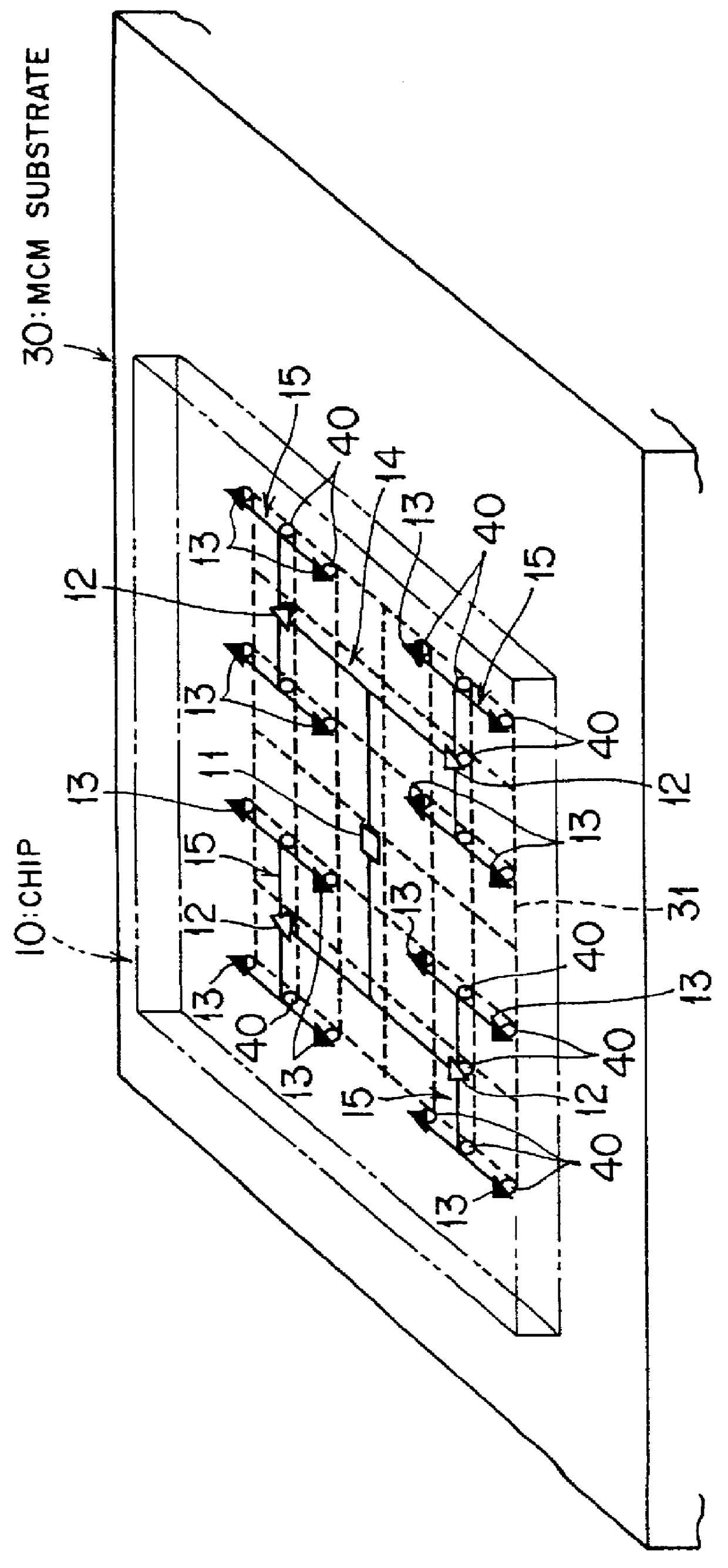
FIG. 1 is a perspective view schematically showing a clock distribution circuit in a semiconductor integrated circuit according to the invention. In FIG. 1, a main portion of the clock distribution circuit is illustrated as viewed at an angle from above in a perspective manner.

As shown in FIG. 1, according to the first embodiment, there are provided on a square chip (e.g., a semiconductor integrated circuit) 10 a first-stage driver 11 for receiving a clock signal from the outside of the chip, four second stage drivers 12 for receiving an output from the first stage driver 11; and sixteen third-stage drivers (drivers in the final stage) 13 for receiving outputs from the second-stage drivers 12.

The drivers 11 to 13 are arranged on the chip in the same manner as those arranged under the H-tree clock distribution method shown in FIG. 4.

More specifically, the first-stage driver 11 is disposed on the center of the chip 10, and the first-driver 11 is further connected to the four second-st...

second embodiment

[B] Description of a Second Embodiment

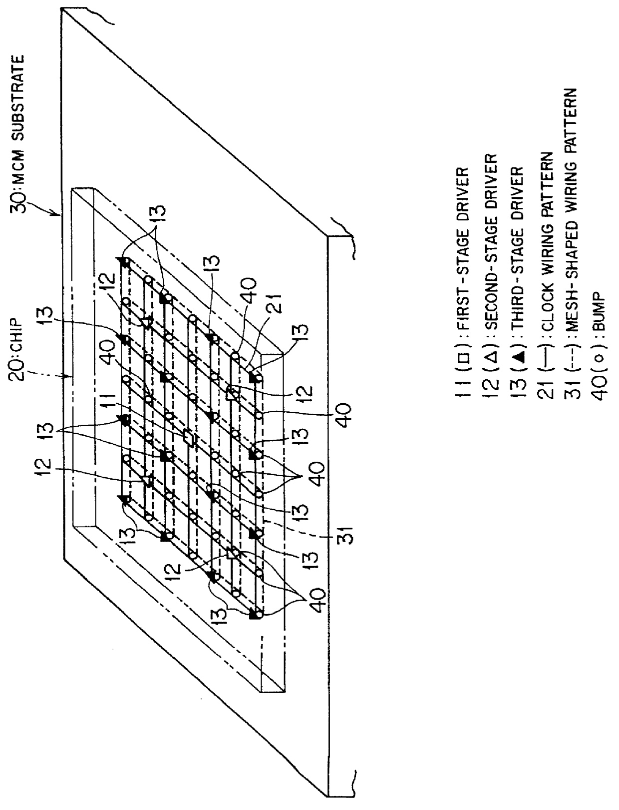
FIG. 3 is a perspective view schematically showing a clock distribution circuit in a semiconductor integrated circuit according to a second embodiment of the present invention. In FIG. 3 as well, a main portion of the clock distribution circuit is illustrated as viewed at an angle from above in a perspective manner.

As show in FIG. 3, in the second embodiment as well, there are provided on a square chip (e.g., a semiconductor integrated circuit) 20 the first-stage driver 11 for receiving a clock signal from the outside of the chip, the four second-stage drivers 12 for receiving an output from the first-stage driver 11; and the sixteen third-stage drivers (drivers in the final stage) 13 for receiving outputs from the second-stage drivers 12.

In the second embodiment, the drivers 11 to 13 are disposed on the chip in the same manner as those arranged under the clock distribution method shown in FIG. 5.

More specifically, the first-stage driver 11 is d...


PUM


Abstract

A clock distribution circuit reliably reduces clock skew, while preventing the waveform of a clock signal from rounding, which would otherwise occur due to an increase in resistance, and preventing instability of the clock signal, which would otherwise occur due to an increase in inductance, thereby realizing ideal clock distribution. In the clock distribution circuit, a clock wiring pattern for distributing the clock signal is formed on a chip, and a wiring pattern whose resistance is lower than the clock wiring pattern is formed on a substrate, on which the chip is mounted, in such a way as to be connected to the clock wiring pattern at a plurality of locations. The clock distribution circuit is applied to semiconductor integrated circuits such as LSIs built in multichip modules.

Description

1) Field of the InventionThe present invention relates to a clock distribution circuit which distributes a clock signal to a plurality of cells having clock terminals in a semiconductor integrated circuit in which the plurality of cells are formed on a chip, and more particularly to a clock distribution circuit suitable for use in a semiconductor integrated circuit, such as an LSI, to be incorporated into a multichip module (hereinafter often abbreviated as "MCM").2) Description of the Related ArtGenerally, in the case of a semiconductor integrated circuit, e.g., an LSI, the overall LSI is operated in synchronism with a clock signal or a plurality of clock signals which are out of phase with one another. In such a case, the clock signal received from the outside of the circuit is distributed to flip-flops and the like (cells having clock terminals), in respective parts of the LSI, whereby decoding operations, reading or writing of memory, or various arithmetic operations are perform...

Claims


Application Information

Patent Timeline
IPC IPC(8): G06F1/10H03K19/003H03K5/15
CPCG06F1/10H03K19/00323
Inventor ISHIZAKA, KINYA
Owner FUJITSU LTD
Why Eureka
Try Eureka