Eureka AIR delivers breakthrough ideas for toughest innovation challenges, trusted by R&D personnel around the world.

Predriver logic circuit

a logic circuit and pre-driver technology, applied in logic circuits, voltage/current interference elimination, reliability increasing modifications, etc., can solve the problems of reducing the timing margin at the receiver, reducing the timing margin, and simultaneous switching output nois

Inactive Publication Date: 2000-03-28
INTEL CORP
View PDF6 Cites 27 Cited by
  • Summary
  • Abstract
  • Description
  • Claims
  • Application Information

AI Technical Summary

Problems solved by technology

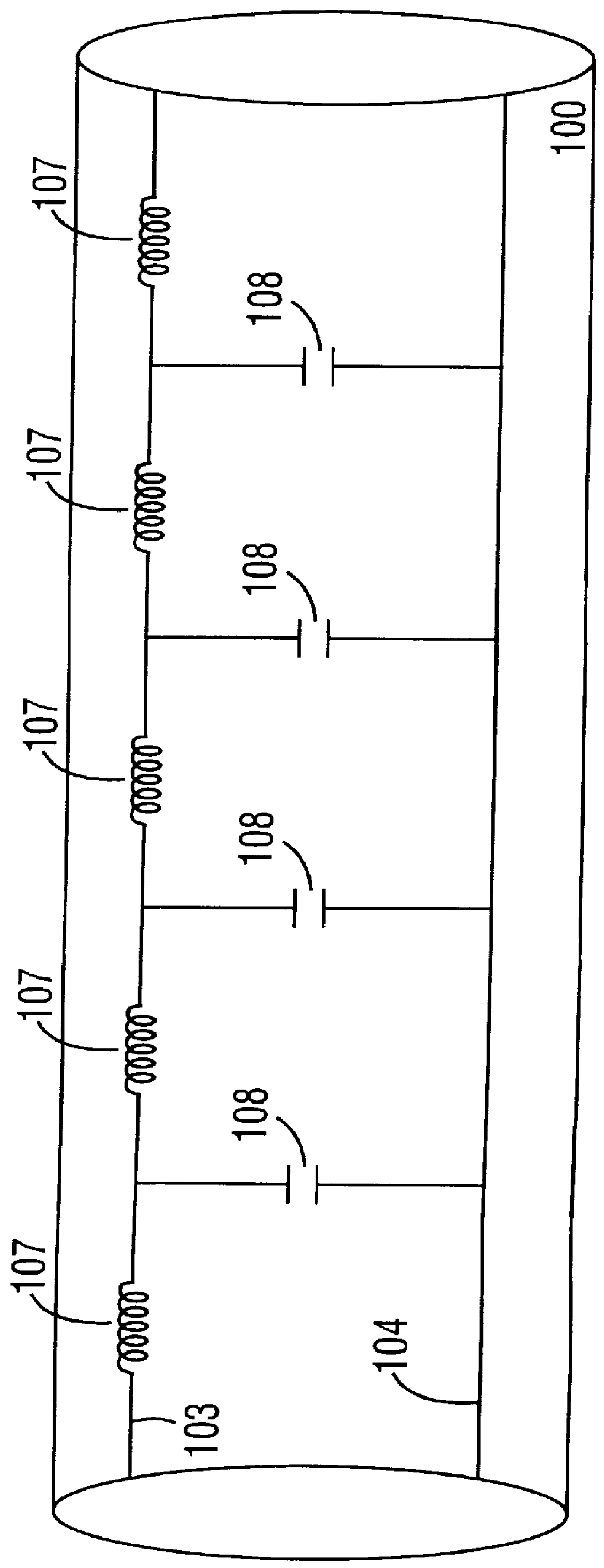
If a fast RC charge rate is chosen, the driver circuit 205 is charged extremely fast, which may result in simultaneous switching output noise (i.e., ground bounce).
Ground bounce generally causes additional propagation delays in the output signal thereby reducing the timing margin at the receiver.
Distortion in the shape of the signal may also result from ground bounce.
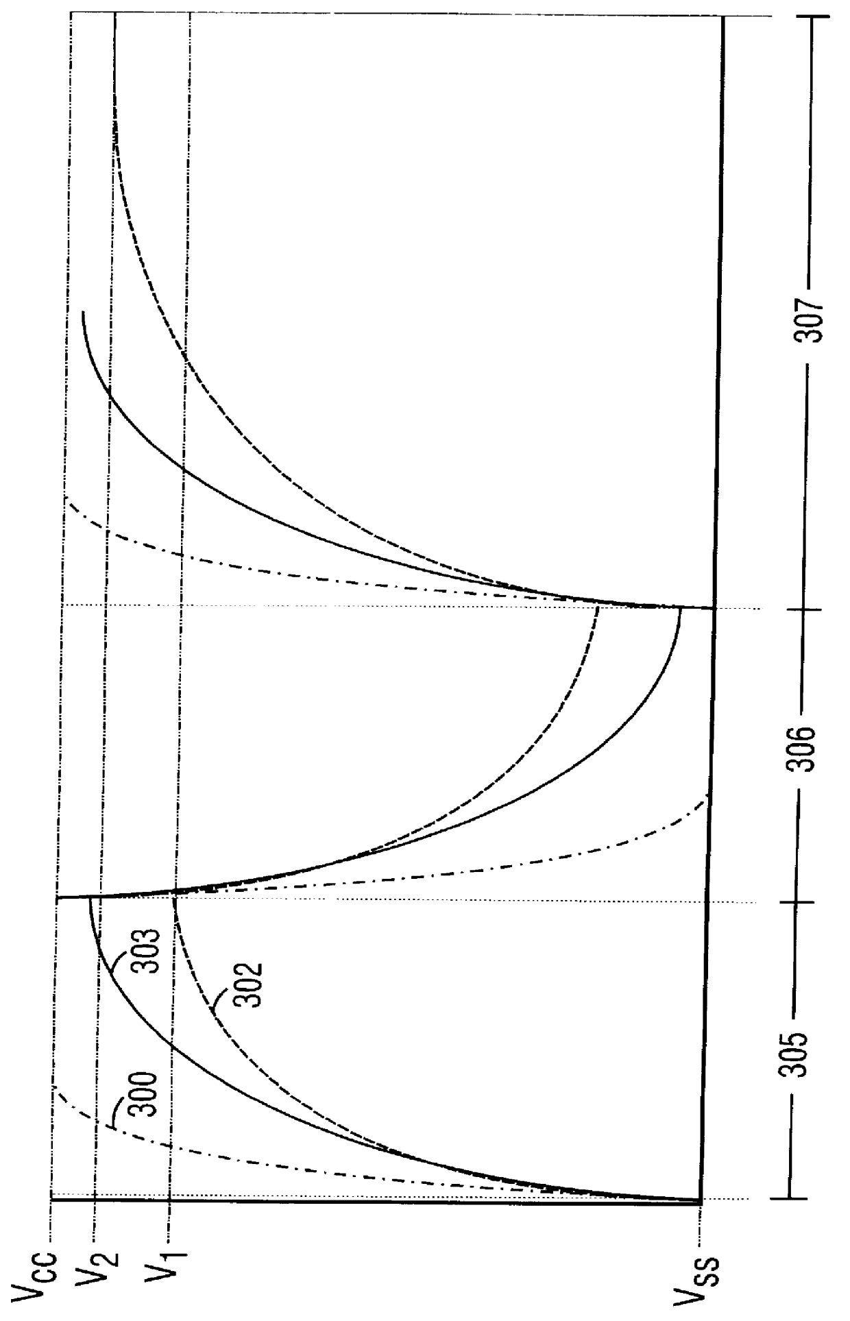
The charging to different voltage levels for the same state may cause the driver circuit to behave differently (e.g., the line may take longer to settle).
This aberrant behavior may vary the timing requirements for proper operation and affect signal quality.
Though the ground bounce at this rate is considerably lower, the ground bounce is still present and may lead to false logic signals.
Similarly, though the amount of data pattern dependent charging is considerably lower, it is still present, which may impact signal quality, among other things.

Method used


Image

  • Predriver logic circuit
  • Predriver logic circuit
  • Predriver logic circuit

Examples


first embodiment

A First Embodiment

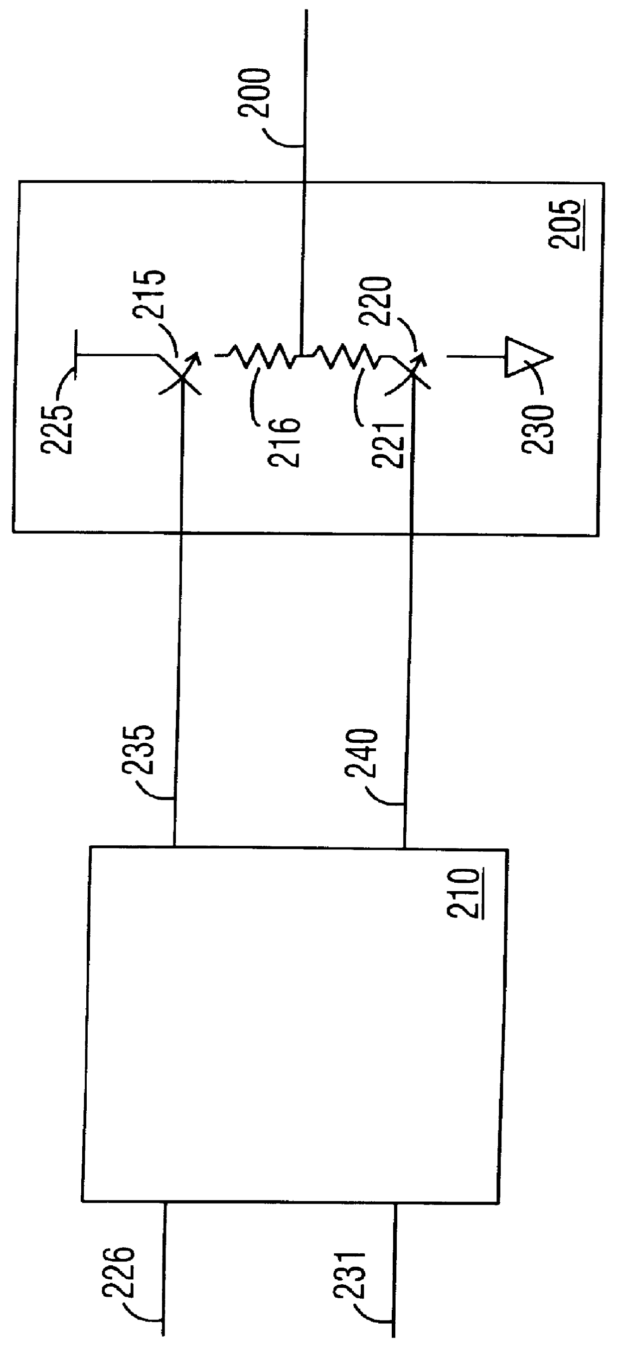
FIG. 5A is a circuit diagram for a first embodiment of the predriver circuit 410 that is coupled to the transmission line 400 through the driver circuit 405. The driver circuit 405 has two complementary metal oxide semiconductor (MOS) transistors 414, 415 that function essentially as switches. One skilled in the art will appreciate that the transistors 414, 415 may be replaced by any transistor topology allowing for complementary transistors (e.g., bipolar transistors and field effect transistors). The PMOS transistor 415 has a source terminal coupled to the reference voltage supply 417, a gate terminal coupled to the predriver circuit 410 by the line 419, and a drain terminal coupled to the transmission line 400. The voltage level of the signal applied to the line 419 is used to enable (i.e., turn "on") the transistor 415. Enabling the transistor 415 allows current to flow from the source to the drain such that a supply voltage (e.g., V.sub.CC) may be applied to t...

second embodiment

A Second Embodiment

FIG. 6 is a circuit diagram of a second embodiment of the predriver circuit 410 in accordance with the invention. The output PMOS network 420 and output NMOS network 430 include pulse generators 624, 634 coupled to the logic circuits 424, 434, respectively. Each of these pulse generators have two input terminals 625, 626; 635, 636 on which a data signal and an enable signal may be applied. The pulse generators 624, 634 may be used to enable the logic circuits 424, 434 for a predetermined amount of time. The predetermined period of time may be designed to correspond to the time that it takes to charge the gates of transistors 414, 415 to the appropriate threshold voltage.

Once this time has been determined, a pulse may be emitted by the pulse generators 624, 634 that has a duration corresponding to this threshold charge time. The specifics regarding pulse generation have not been included so as not to obscure the present invention. Rather, the relationship of the pu...


PUM


Abstract

A buffer for enabling a signal to be applied to a bus. The buffer includes a first transistor coupled to a bus and a voltage supply. The logic buffer includes a first logic circuit which has an input coupled to receive a data signal and adapted to charge a terminal of the transistor at a first rate in response to a transition in the data signal. A second logic circuit charges the terminal at a faster rate during an initial transition period, until a first preselected condition is met. The buffer also includes a third logic circuit to charge the terminal at a second faster rate during a final transition period, after a second preselected condition is met. A method for controlling a voltage level of a signal applied to a terminal of a transistor includes charging the terminal at a fast rate until a first preselected condition is met. The terminal is then charged at a slower rate, until a second preselected condition is met, at which time the terminal is charged at a second fast rate, which is also greater than the slower rate.

Description

1. Field of the InventionThe invention relates in general to the field of logic circuits, and, more particularly, to logic circuits used in computer systems. Specifically, the invention relates to a predriver logic circuit to improve the output characteristics of a driver circuit for a bus.2. Description of the Related ArtModem computer systems may contain several microprocessors, micro-controllers, and other digital devices connected to each other by a bus. The bus transports data among the microprocessors and other components and is composed of a number of traces. Traces are wire-like connections that are printed on a circuit board and function as transmission lines.In most modem computer systems, data is in the form of bits (i.e., binary digits). Bits are typically represented as voltages. When positive logic is used, a bit value of one (i.e., a logic one) is generally represented as a high voltage, while a bit value of zero (i.e., a logic zero) is generally represented as a low ...

Claims


Application Information

Patent Timeline
IPC IPC(8): H03K19/003
CPCH03K19/00361
Inventor DABRAL, SANJAYSAMPATH, DILIP K.ILKBAHAR, ALPER
Owner INTEL CORP
Why Eureka
Eureka Blog
Learn More