Semiconductor device having capacitor

a technology of semiconductor devices and capacitors, which is applied in the direction of semiconductor devices, capacitors, electrical equipment, etc., can solve the problems of deterioration of electric characteristics, increase of leakage current, and serious problems such as the inability to meet the requirements of the application, and achieve the effect of improving the scale of integration

Inactive Publication Date: 2000-04-04
PANASONIC CORP
View PDF9 Cites 8 Cited by
  • Summary
  • Abstract
  • Description
  • Claims
  • Application Information

AI Technical Summary

Benefits of technology

Besides, by disposing a third hole in the capacitor insulating layer, the region near the end portion of the top electrode can be utilized as the hole region for interconnections, so that the capacitor may be further advanced in the scale of integration.

Problems solved by technology

At the same time, as the consumer electronic appliances are becoming higher in density, unwanted radiation which is electromagnetic noise released from electronic appliances is posing a serious problem.
In such conventional structure, however, the following problems occur.
Therefore, in the conventional structure in which the capacitor insulating layer 8 and top electrode 9 are identical in shape, the degraded crystallinity portion is contained in the capacitor, and it is likely to cause deterioration of electric characteristics, such as drop of capacitance, increase of leakage current, and drop of dielectric strength.

Method used


Image

  • Semiconductor device having capacitor
  • Semiconductor device having capacitor
  • Semiconductor device having capacitor

Examples


first embodiment

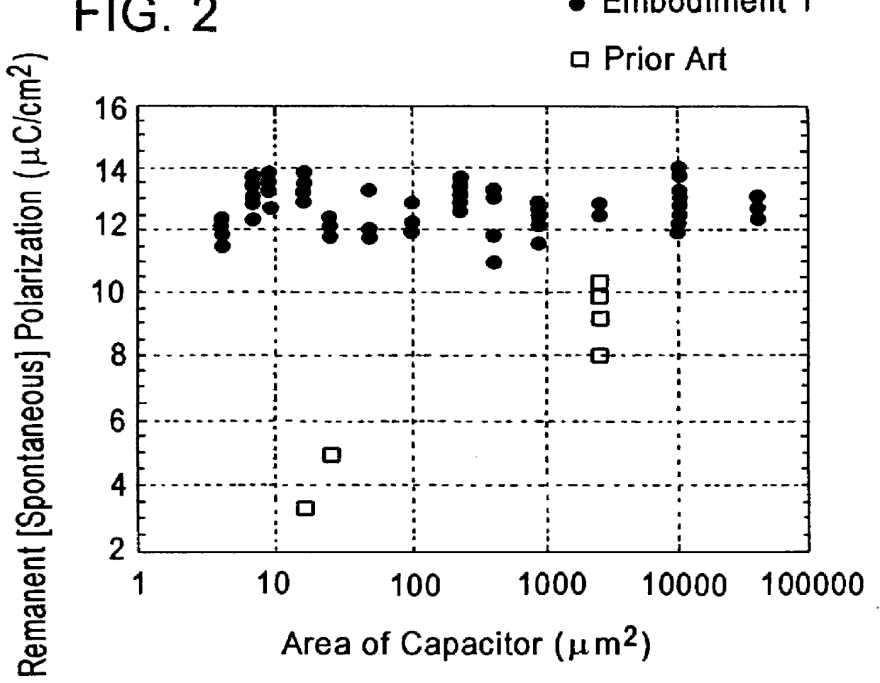
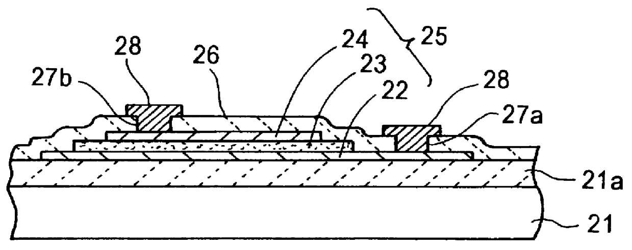
FIG. 1 is a sectional view of a capacitor portion of a semiconductor device in the invention. However, the region in which the integrated circuit element is formed is same as in the prior art shown in FIG. 6, and is hence omitted in the drawing.

As shown in FIG. 1, a bottom electrode 22 of platinum in a thickness of 100 to 300 nm is formed on an insulating layer 21a formed on a semiconductor substrate 21. On the bottom electrode 22, a capacitor insulating layer 23 of SrBi.sub.2 Ta.sub.2 O.sub.9 having lamellar structure in a thickness of 50 to 250 nm, smaller in area than the bottom electrode 22, is formed. The end portion of the capacitor insulating layer 23 is positioned inside of the end portion of the bottom electrode 22. On the capacitor insulating layer 23, a top electrode 24 of platinum in a thickness of 100 to 300 nm, smaller in area than the capacitor insulating layer 23, is formed. The end portion of the top electrode 24 is positioned inside of the end portion of the capaci...

second embodiment

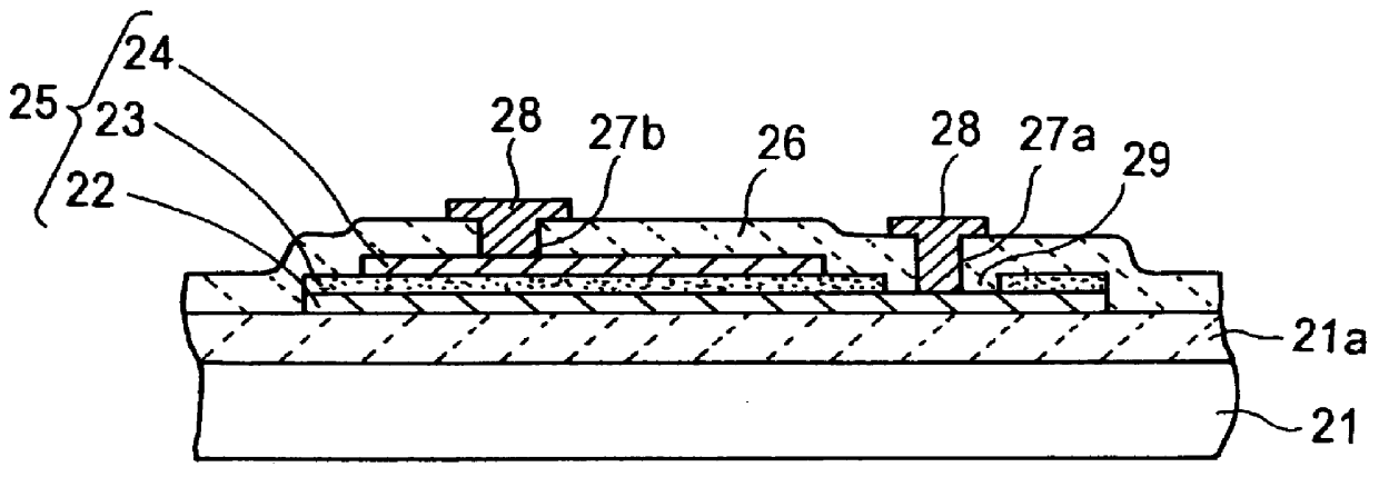
The dimensional relation of the capacitor insulating layer 23 and bottom electrode 22, and the position relation of the end portions may be also the relations as shown in FIG. 4 and FIG. 5. In FIG. 4, the capacitor insulating layer 23 and bottom electrode 22 are same in size, and both are disposed at the same position. In FIG. 5, the capacitor insulating layer 23 is larger than the bottom electrode 22, and the end portion of the capacitor insulating layer 23 is projecting from the end portion of the bottom electrode 22. In either case, the end portion of the capacitor insulating layer 23 is outside of the end portion of the top electrode 24, and hence the same effects as in the second embodiment are obtained.

The invention is not limited to the illustrated embodiments alone, and various modifications are possible. For example, in the foregoing embodiments, platinum films are used as the bottom electrode and top electrode of the capacitor, but the platinum films may be also replaced b...


PUM


Abstract

A capacitor 25 is formed on an insulating layer 21a formed on a semiconductor substrate 21. The end portion of a capacitor insulating layer 23 is positioned between the end portion of a bottom electrode 22 and the end portion of a top electrode 24. A passivation layer 26 for covering the capacitor 25 is formed. Interconnections 28 are connected to the bottom electrode 22 through a first hole 27a and to the top electrode 24 through a second hole 27b. In this way, since the end portion of the capacitor insulating layer 23 is out of the end portion of the top electrode 24, the end portion of the capacitor insulating layer 23 injured by etching does not affect the capacitance.

Description

BACKGROUND OF THE INVENTIONThe present invention relates to a semiconductor device having a capacitor using a ferroelectric layer or dielectric layer having high permittivity as a capacitor insulating layer.Recently, to realize a nonvolatile RAM of low operating voltage and capable of writing / reading at high speed never known before, technical developments are intensively attempted to form a capacitor using a ferroelectric layer having spontaneous polarization as a capacitor insulating layer, on a semiconductor integrated circuit. At the same time, as the consumer electronic appliances are becoming higher in density, unwanted radiation which is electromagnetic noise released from electronic appliances is posing a serious problem. As the measure to reduce the unwanted radiation, a keen attention has been concentration on the technology of incorporating a capacitor of large capacitance using a ferroelectric layer or a dielectric layer having high permittivity (these layers are commonl...

Claims


Application Information

Patent Timeline
Patent Type & Authority Patents(United States)
IPC IPC(8): H01L29/66H01L29/92H01L27/04H01L21/822H01L21/8242H01L21/8246H01L27/10H01L27/105H01L27/108
CPCH01L28/40H01L27/04
Inventor ARITA, KOJIMATSUDA, AKIHIRONAGANO, YOSHIHISANASU, TORUFUJII, EIJI
Owner PANASONIC CORP
Why Eureka
Try Eureka