Integrated circuit design based on scan design technology

a scan design and integrated circuit technology, applied in the field of design for testability technology based on scan design, can solve the problems of useless power consumption, insufficient power consumption, insufficient power consumption of inoue's approach, etc., and achieve the effect of enhancing the power consumption reduction effect for the entire chip, reducing the power consumption of the dummy block, and increasing the number of integrated dummy blocks

Inactive Publication Date: 2009-02-05
RENESAS ELECTRONICS CORP
View PDF3 Cites 209 Cited by
  • Summary
  • Abstract
  • Description
  • Claims
  • Application Information

AI Technical Summary

Benefits of technology

[0014]The dummy block(s) finally left in the final product chip receives the clock signal, but operates not responsively to the clock signal. Therefore, the power consumption of the dummy block is largely reduced, compared with the case where dummy cells of the same configuration as normal scan flip-flop cells are used. The effect of power consumption reduction for the entire chip is enhanced with the increase in the number of integrated dummy blocks. Therefore, the power consumption reduction effect is promoted with the increase in the scale of the integrated circuit accompanied by the advance of the fine processing technology.
[0015]The approach of this invention does not require a clock gating circuit through which a clock signal is fed to the dummy blocks. This avoids chip resource waste, making effective use of chip resources. As a result, the chip size is reduced.

Problems solved by technology

One issue is that the clock supply may be unbalanced when a clock line is newly connected to a spare scan flip-flop cell in the design change.
According to the inventor's study, however, the Inoue's approach suffers from useless increase in the power consumption.
This leads to useless power consumption.
However, the additionally-provided clock gating circuit requires the chip resource and increases the chip size.

Method used


Image

  • Integrated circuit design based on scan design technology
  • Integrated circuit design based on scan design technology
  • Integrated circuit design based on scan design technology

Examples


Embodiment Construction

[0028]The invention will be now described herein with reference to illustrative embodiments. Those skilled in the art will recognize that many alternative embodiments can be accomplished using the teachings of the present invention and that the invention is not limited to the embodiments illustrated for explanatory purposes.

Circuit Design Procedure

[0029]In one embodiment of the present invention, an integrated circuit design procedure based on a design-for-testability technique is provided. In this design procedure, scan flip-flop cells are used to implement a scan test.

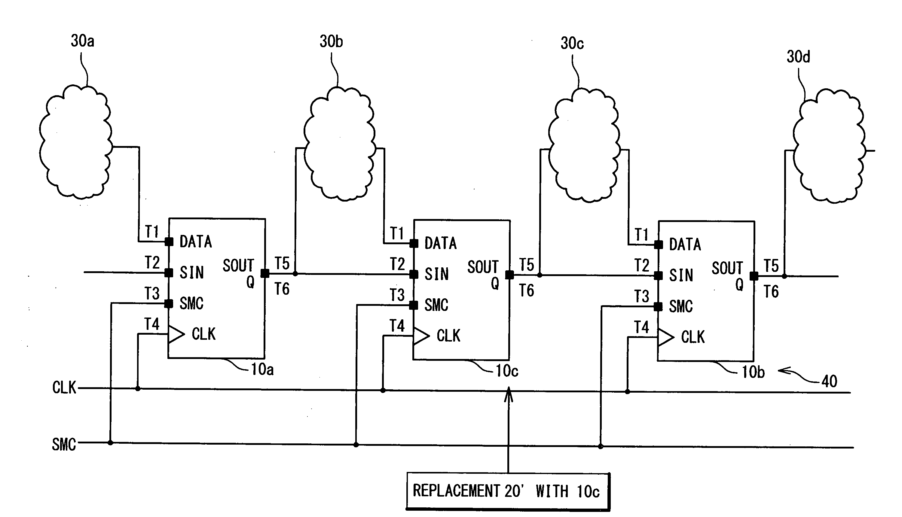
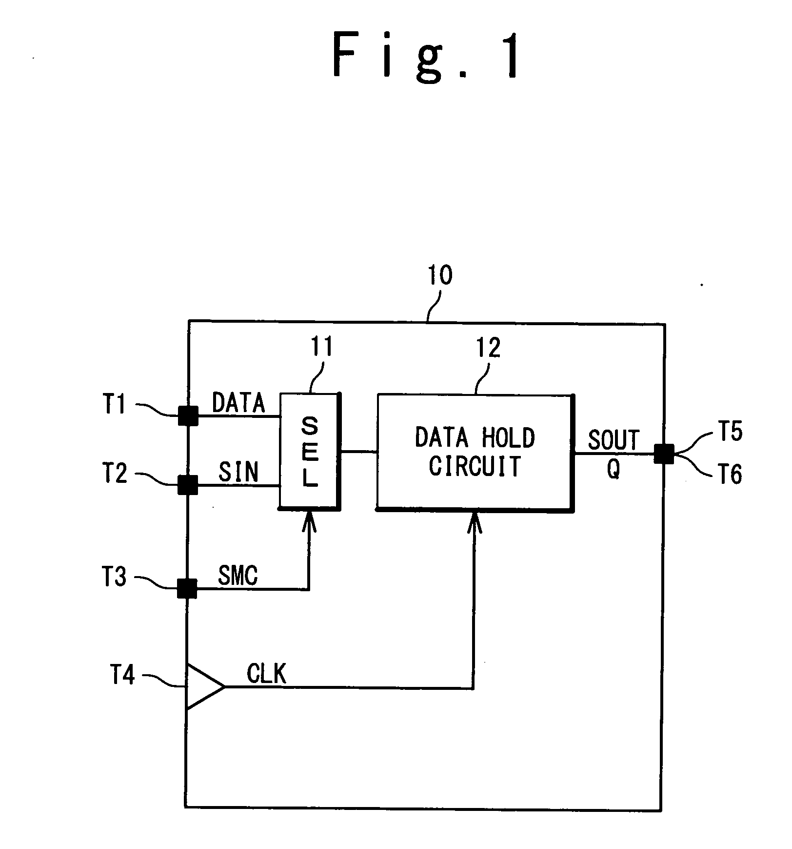
[0030]FIG. 1 schematically shows an exemplary configuration of scan flip-flop cells 10 used in this embodiment. The scan flip-flop cells 10 each have a data input terminal T1, a scan input terminal T2, an SMC (Scan Mode Control) terminal T3, a clock terminal T4, a scan output terminal T5 and a data output terminal T6. The data input terminal T1 and the data output terminal T6 are terminals connected to data signal li...


PUM


Abstract

An integrated circuit is provided with a scan chain including a scan flip-flop and a dummy block. The dummy block has a clock terminal receiving a clock signal, a scan input terminal connected to a scan data line within the scan chain, and a scan output terminal connected to another scan data line within the scan chain. The dummy block is configured to output data on the scan output terminal in response to input data fed to the scan input terminal, not responsively to the clock signal.

Description

INCORPORATION BY REFERENCE[0001]This application claims the benefit of priority based on Japanese Patent Application No. 2007-198617, filed on Jul. 31, 2007, the disclosure of which is incorporated herein by reference.BACKGROUND OF THE INVENTION[0002]1. Field of the Invention[0003]The present invention relates to a semiconductor integrated circuit and a method of designing the same. More particularly, the present invention relates to a design-for-testability technology based on scan design.[0004]2. Description of the Related Art[0005]Semiconductor integrated circuits are tested after the manufacture to detect malfunctions of the circuits, such as delay faults and stuck-at faults. One known integrated circuit design technique for improving testability is to incorporate test circuits into the circuits to be designed. Such design technique is often referred to as design for testability (DFT).[0006]The scan design is one of the known design-for-testability techniques. In a semiconductor...

Claims


Application Information

Patent Timeline
Patent Type & Authority Applications(United States)
IPC IPC(8): H01L27/00G06F17/50
CPCG06F17/5059G06F17/505G06F30/327G06F30/35
Inventor IRIE, KAZUYUKI
Owner RENESAS ELECTRONICS CORP
Why Eureka
Try Eureka