Hidden precharge pseudo cache DRAM

a pseudo-cache and pre-charge technology, applied in the field of dram, can solve the problems of affecting the use the freedom of computer system designers to exploit, and the inability to use the approach of the home p

Inactive Publication Date: 2000-05-09
TAIWAN SEMICON MFG CO LTD
View PDF9 Cites 42 Cited by
  • Summary
  • Abstract
  • Description
  • Claims
  • Application Information

AI Technical Summary

Problems solved by technology

The technology of the home PC becomes more complicated than the traditional business PC, which provides only the office productivity.
CPU is currently dominated by Intel Corp., and most of the computer system designers do not have much freedom to exploit in this area.
The approach usually becomes prohibited in the home PC because of the high cost of cache Static Random Access Memory (SRAM).
But the cacheless system may cost the performance degradation from 20% up to 50%.
The new DRAM technology like Extended Data Out(EDO) DRAM can only improve performance by less than 5%.
Even Burst-EDO(BEDO), Synchronous DRAM or RAMBUS DRAM can only improve performance by less than 10%.
None of current DRAM technologies can really solve the problem of performance degradation when cache memory is not implemented within the system.
The reason for the minor improvement with those new DRAM technologies is due to the fact of bad memory locality in the behavior of 32-bit operating system.
The bad memory locality causes a huge overhead both to the cache-miss rate and DRAM page-miss rate.
But this approach will yield a bigger die size due to inefficient overhead of its peripheral circuits.
As a result, the cost of current new type DRAMs, which are implemented intentionally to replace the cache SRAM in the computer system, may easily exceeds the cost of cache SRAM.
Therefore, low cost and, at the same time, high performance is simply not available from the conventional wisdom up to date.

Method used


Image

  • Hidden precharge pseudo cache DRAM
  • Hidden precharge pseudo cache DRAM
  • Hidden precharge pseudo cache DRAM

Examples


Embodiment Construction

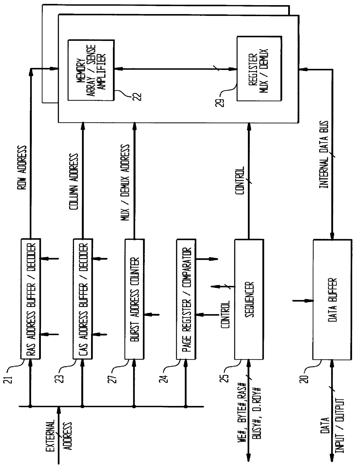
A HPPC DRAM architecture of the invention is shown in FIG. 1. It contains one row address buffer / decoder 21 (RAS buffer / decoder) and one column address buffer / decoder 23 (CAS buffer / decoder).

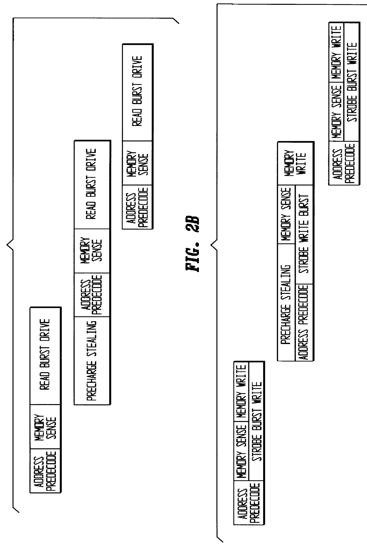
Both RAS buffer / decoder 21 and CAS buffer / decoder 23 simultaneously decode the address for both pending cycle and on-going cycle. Thus it allows the external memory controller (not shown) to achieve high performance pipeline access. As hereinafter recited, an internal sequencer 25 controls the timing of operation of the two address buffers / decoders and other circuits to achieve a pipeline timing chain. In such arrangement, the critical timing path of DRAM access time can be partitioned and the sequencer 25 performs memory burst cycle pipeline operation.

The HPPC DRAM includes a burst address counter 27 which is a loadable counter. Whenever the sequencer 25 loads a new column address to CAS buffer / decoder 23, A1 and A0 bits of the address value is loaded to the burst address counter 27 as the init...


PUM


Abstract

A new DRAM architecture, HPPC DRAM, is provided to support a high performance and low cost memory system. The HPPC DRAM has integrated the following concepts into a single DRAM chip. First, superset pin definitions backward-compatible to the traditional fast-page-mode DRAM SIMM. This allows one memory controller to support a memory system having both a traditional fast-page-mode DRAM and HPPC DRAM of this invention. Secondly, combining a memory array, a register of 4:1 Mux/Demux function, a RAS buffer/decoder, a CAS buffer/decoder, a burst address counter, a page register/comparator, a sequencer and a data buffer into a single DRAM IC chip. Using these intelligent peripheral circuits, the HPPC DRAM execute a pipeline cycle request and precharge cycle stealing. Thirdly, a precharge cycle stealing pipeline is implemented to the timing chain of read operation to eliminate the precharge cycle time which is achieved by executing read drive concurrently to the precharge cycle. This read timing chain shows that a zero wait state is sustained if there is a page-hit. Fourthly, a precharge cycle stealing pipeline is implemented to the timing chain of write operation to eliminate the precharge cycle time which is achieved by executing precharge cycle concurrently to address predecoding and data strobing.

Description

TECHNICAL FIELD OF INVENTIONThe invention relates to Dynamic Random Access Memory (DRAM) and, in particular, to DRAM with characteristics of hidden precharge.TECHNICAL BACKGROUND OF INVENTIONIn recent years, the home PC has the highest growth rate in the PC market. The home PC provides not only the personal productivity enhancement but also communication, entertainment and education. The technology of the home PC becomes more complicated than the traditional business PC, which provides only the office productivity. Facing the introduction of 32-bit Windows 95 operating system, the design of home PC is no longer a trivial job to most computer designers. Take an example of the following challenge: home PC needs not only a very low cost structure to be mass manufactured but also a very high performance to run various applications. The key components of PC are consisted of four parts, namely CPU, memory, system core logic and peripheral subsystem. CPU is currently dominated by Intel Cor...

Claims


Application Information

Patent Timeline
Patent Type & Authority Patents(United States)
IPC IPC(8): G06F12/08G11C11/406G11C11/401
CPCG11C11/406G06F12/0893
Inventor GUO, TA-PEN
Owner TAIWAN SEMICON MFG CO LTD
Why Eureka
Try Eureka