Blanket-selective chemical vapor deposition using an ultra-thin nucleation layer

a chemical vapor deposition and ultra-thin technology, applied in chemical vapor deposition coating, conveyor parts, resistive material coating, etc., can solve the problems of void in the filled aperture, width of the aperture, and association with blanket cvd process

Inactive Publication Date: 2000-05-23
APPLIED MATERIALS INC
View PDF26 Cites 61 Cited by
  • Summary
  • Abstract
  • Description
  • Claims
  • Application Information

AI Technical Summary

Problems solved by technology

However, there are two primary difficulties associated with blanket CVD processes.
First, blanket CVD films grow from all sides in an aperture which typically results in a void in the filled aperture because the deposited layer grows upwardly and outwardly at the upper corners of the aperture and bridges at the upper surface of the aperture before the aperture has been completely filled (i.e., "crowning").
Also, a nucleation layer, i.e., a continuous film layer to insure nucleation over all surfaces of the substrate, which must be deposited on the aperture walls to ensure deposition of the CVD layer thereon further reduces the width of the aperture, thereby increasing the difficulty of void-free filling of the aperture wit

Method used


Image

  • Blanket-selective chemical vapor deposition using an ultra-thin nucleation layer
  • Blanket-selective chemical vapor deposition using an ultra-thin nucleation layer
  • Blanket-selective chemical vapor deposition using an ultra-thin nucleation layer

Examples


Embodiment Construction

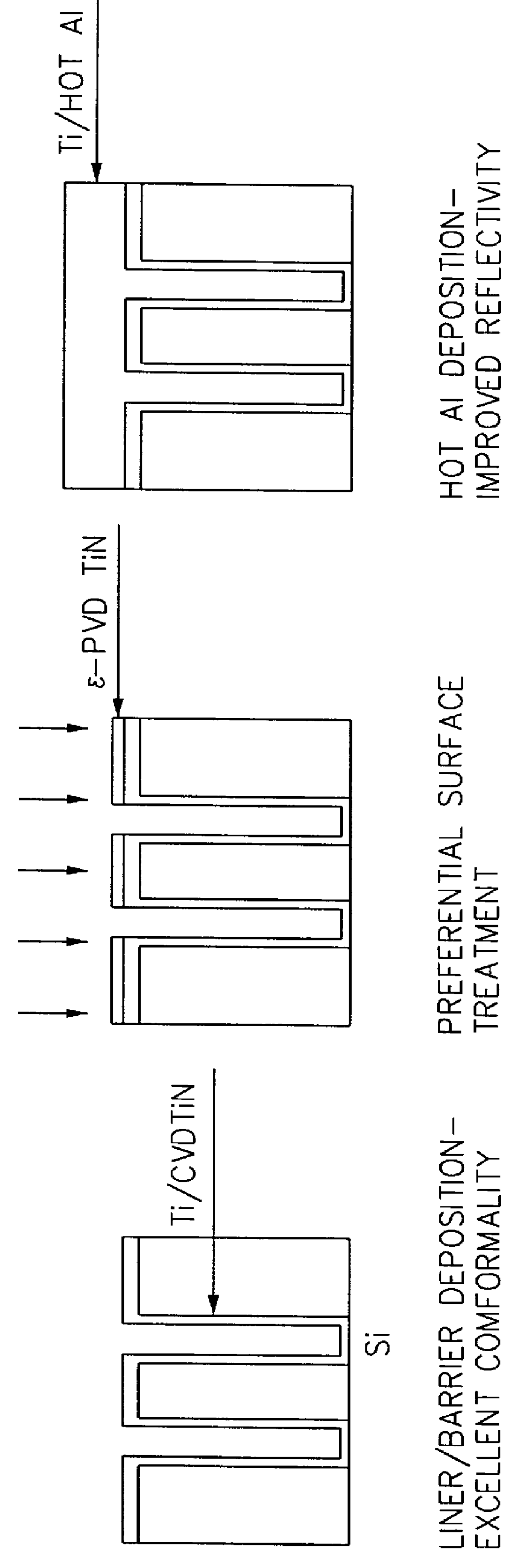
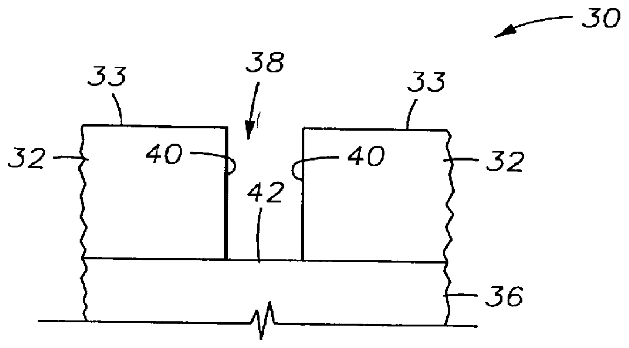
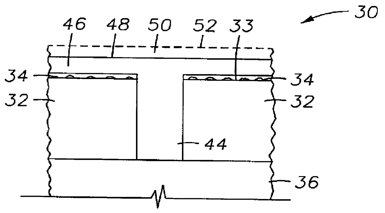
The present invention provides a method and apparatus for obtaining film layers with highly oriented crystal structures having improved reflectivity, wherein the ultimate layer is formed by either CVD or PVD techniques. The present invention also provides a process and apparatus for the selective deposition of material within small geometries, such as high aspect ratio apertures, which will selectively form void-free structures such as interconnects in the apertures while also forming a matching film layer on the field. In one aspect of the invention, this is provided by depositing a small quantity of refractory material, preferably TiN, on the surface of the substrate and then forming a conducting film layer thereon. In another aspect of the invention, nucleation sites are formed on the field by depositing the small quantity of refractory material on the field which, when exposed to the chemical vapor, initiate film growth which provides a film layer thereon which does not bridge t...


PUM

PropertyMeasurementUnit
Angleaaaaaaaaaa
Angleaaaaaaaaaa
Angleaaaaaaaaaa

Abstract

The present invention relates generally to an improved apparatus and process for providing uniform step coverage on a substrate and planarization of conducting layers to form continuous, void-free interconnects in sub-half micron, high aspect ratio aperture width applications and highly oriented conducting layers. In one aspect of the invention, a dielectric layer is formed over a conducting or semiconducting layer and etched to form an aperture exposing the underlying conducting or semiconducting layer on the aperture floor. An ultra-thin nucleation layer is then deposited by physical vapor deposition onto the field of the dielectric layer. A CVD metal layer is then deposited onto the structure to achieve selective deposition on the floor of the aperture, while preferably also forming a highly oriented blanket layer on the field. The present apparatus and process reduce the number of steps necessary to fabricate CVD metal interconnects and layers that are substantially void-free and planarized. The metallization process is preferably carried out in an integrated processing system that includes both a PVD and CVD processing chamber so that once the substrate is introduced into a vacuum environment, the metallization of the apertures to form vias and contacts occurs without the formation of oxides between the layers.

Description

The present invention relates to a method and apparatus for manufacturing integrated circuits on semiconductor substrates. More particularly, the present invention relates to the deposition of a nucleation layer on a substrate and subsequently depositing a conducting layer thereon resulting in a highly oriented crystal structure within this subsequent layer having improved electromigration performance. In another aspect of the invention, a method and apparatus is provided for the selective metallization of apertures formed on substrates in the fabrication of integrated circuits to form void-free interconnects between conducting layers, including apertures such as contacts or vias in high aspect ratio sub-half micron applications, while preferably also forming a highly oriented blanket layer on the field.BACKGROUND OF THE RELATED ARTSub-half micron multilevel metallization is one of the key technologies for the next generation of very large scale integration ("VLSI"). The multilevel ...

Claims


Application Information

Patent Timeline
IPC IPC(8): C23C14/56C23C16/54H01L21/02H01L21/768H01L21/70H01L21/3205H01L21/285H01L21/28H01L21/677
CPCC23C14/568C23C16/54H01L21/32051H01L21/76879H01L21/76876H01L21/76877H01L21/76843
Inventor GUO, TEDCHEN, LIANGCHEN, FUSENMOSELY, RODERICK C.
Owner APPLIED MATERIALS INC
Why Eureka
Try Eureka