Method and apparatus for detecting soft errors in content addressable memory arrays

a technology of addressable memory array and soft error detection, which is applied in the field of methods and apparatus for detecting soft errors in content addressable memory arrays, can solve problems such as system failure, soft errors may occur in cam arrays, and modern cam arrays are more susceptible to soft errors induced by alpha particles and cosmic rays

Inactive Publication Date: 2000-05-23
INTEL CORP
View PDF5 Cites 87 Cited by
  • Summary
  • Abstract
  • Description
  • Claims
  • Application Information

AI Technical Summary

Problems solved by technology

Nevertheless, soft errors may occur in a CAM array 52 due to the same causes for soft errors occurring in the readable data storage device 14 illustrated in FIG. 1, i.e. impacts of cosmic rays, alpha partic

Method used


Image

  • Method and apparatus for detecting soft errors in content addressable memory arrays
  • Method and apparatus for detecting soft errors in content addressable memory arrays
  • Method and apparatus for detecting soft errors in content addressable memory arrays

Examples


embodiment 111

FIG. 4B illustrates a specific embodiment 111 having two identical CAM memories 100, 112 with duplicate memory locations 108, 109. The parity comparator 105 includes the second CAM array 112 and a hardware device 113. The parity encoder 103 is a group of lines connecting the input source 101 to the second CAM array 112. Pairs of outputs from associated memory locations, e.g., the outputs 106, 115 from the associated memory locations 108, 109, connect to associated input terminals of the hardware device 113. In one embodiment, the hardware device 113 is a bank of AND gates. The inputs of each AND gate connect to one associated pair of outputs. For example, the gate 114 has inputs terminals connected to the output lines 106, 115 from the associated memory locations 108, 109 and an output line 116 to report a "hit." The hardware device 113 delivers a "hit" signal to the output lines 110 in response to an input signal matching the associated copies of the tag word in both CAM arrays 100...

embodiment 120

FIG. 4C is a flowchart illustrating the steps of an embodiment 120 to detect errors, typically soft errors, in the CAM array 100 of FIG. 4A. At block 121, an input signal is compared to tag words stored in the CAM 100 array for a match. At block 122, an output signal is sent from the output lines 106 of the CAM array 100 to the input lines 107 of the parity comparator 105 in response to finding a match between the input data signal and a particular tag word stored in the CAM array 100. At block 123, the output signal from the CAM array 100 enables at least one output line from the parity comparator 105. At block 124, the parity encoder 103 produces a parity signal from the input data signal and sends the parity signal to the input terminal 104 of the parity comparator 105. At block 125, the parity comparator 105 compares the original parity of the particular tag word matching the input signal with the parity signal received from the parity encoder 103. In some embodiments, the parit...

embodiment 139

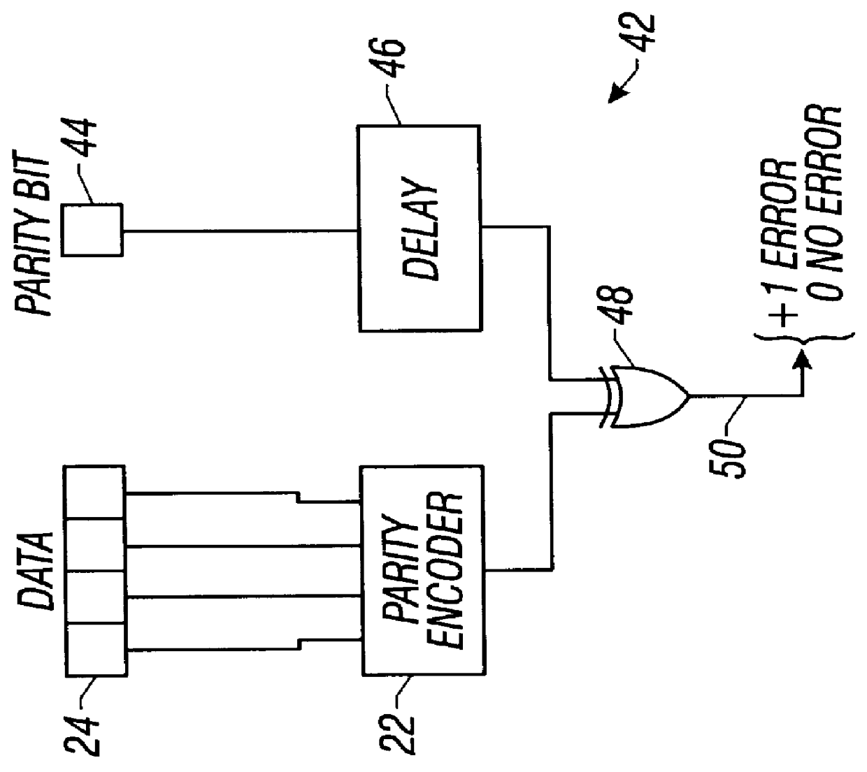
FIG. 5A illustrates a specific embodiment 139 of the parity comparator 105 of FIG. 4A. The parity comparator 105 comprises a CAM parity array 140 and a match detector 141. The CAM parity array 140 may employ SRAM's or dynamic random access memories (DRAM's). The multiple input lines 107 of the parity comparator 105 are connected to multiple first input lines 142 of the match detector 141. Multiple input lines 143 of the CAM parity array 140 are connected in parallel to the input terminal 104 of the parity comparator 105. For each tag memory location of the CAM array 100, there is one or more associated parity memory cells in the CAM parity array 140. For example, the parity memory cell 109 of the CAM parity array 140 is associated with the tag memory location 108 of the CAM array 100. In some embodiments, each memory location of the CAM array 100 has several associated memory cells of the CAM parity array 140, which may be used by error correction codes. Parallel output lines 144 fr...


PUM


Abstract

The invention comprises, in one aspect, a content addressable memory array having a plurality of memory locations to store tag words. The content addressable memory array includes a parity encoder and a parity comparator. The parity encoder has a first input terminal to receive an input data signal and a first output terminal to deliver a signal representative of the parity of the input data signal. The parity comparator has a second input terminal, a third input terminal connected to the first output terminal, and a plurality of memory cells to store original parities of the tag words. The parity comparator compares the original parity of a first tag word to the parity of the input data signal in response to a receiving a match signal. The content addressable memory array includes a fourth input terminal to receive the input data signal, and a second output terminal to send the match signal in response to one of the tag words matching the input data signal. The second output terminal connects to the second input terminal.

Description

1. Field of the InventionThis invention relates generally to computers and memory devices, and, more particularly, to a method and apparatus to detect and correct soft errors in content addressable memory arrays.2. Description of the Related ArtFIG. 1 illustrates one source of soft errors that occasionally occur during the storage or retrieval of binary information, i.e. impacts of cosmic rays and alpha particles on data storage devices. If a cosmic ray or alpha particle 10 crosses a memory location 12 of a semiconductor data storage device or array 14, the value of a binary bit 16 of data stored therein may be changed. The data storage device 14 of FIG. 1 may be a readable memory such as a random access memory. In the example of FIG. 1, the second bit 16 of the memory location 12 has value of logic 1 before the cosmic ray crosses the memory location 12, and the second bit 16 has the value of logic 0 after the cosmic ray 10 crosses therethrough. Several methods and apparatus have be...

Claims


Application Information

Patent Timeline
IPC IPC(8): G06F11/10
CPCG06F11/1064
Inventor RUSU, STEFANFU, JOHN WAI CHEONGTAM, SIMON M.
Owner INTEL CORP
Why Eureka
Try Eureka