Bus interface circuit in a semiconductor memory device
a technology of bus interface circuit and memory device, which is applied in the direction of digital storage, instruments, and increasing the degree of modification of reliability, can solve the problems of power consumption, noise, signal reflection and ringing phenomenon in systems with speeds over 50 mhz, and the limitation of communication at high speed
- Summary
- Abstract
- Description
- Claims
- Application Information
AI Technical Summary
Problems solved by technology
Method used
Image
Examples
first embodiment
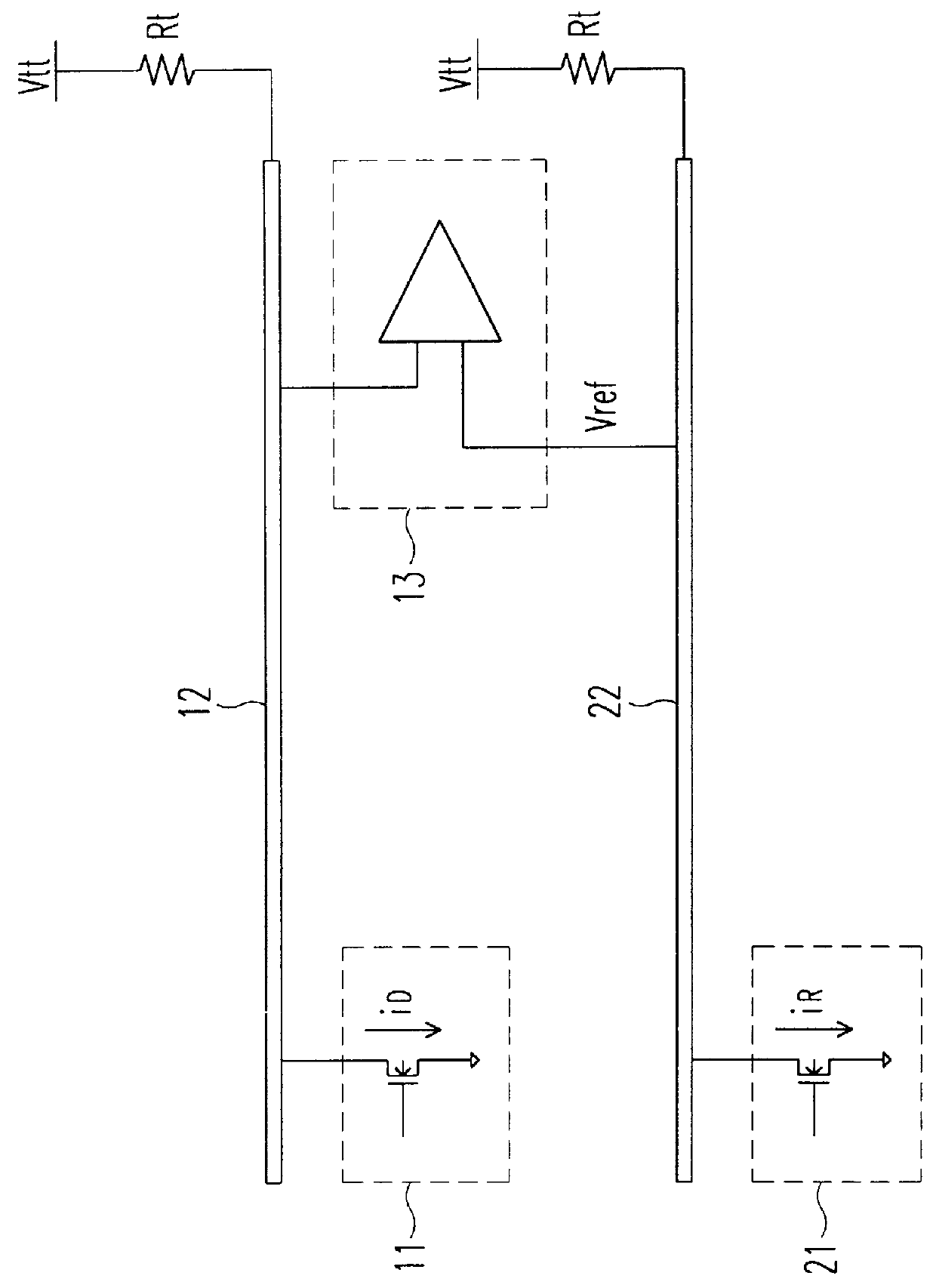
FIG. 2A illustrates a concept diagram of a high-speed bus interface according to the present invention. In FIG. 2A, a bus interface has a data driver 11, a reference voltage driver 21 and a receiver 13. The data driver 11 transmits a data signal through a transmission line 12 that is single terminated. The reference voltage driver 21 transmits a reference voltage signal through a transmission line 22 that is single terminated. The receiver 13 determines logic state by comparing the data signal transmitted through the transmission line 12 with the reference voltage signal transmitted which goes through the transmission line 22.
In the present invention, the reference voltage signal is transmitted to the receiver 13 through a transmission line having identical environment to a transmission line for the data signal, which is different from GTL or RSL interfaces. If the transmission line 12 for the data signal and the transmission line for the reference voltage signal are suitably arrang...
second embodiment
FIG. 4 illustrates a concept diagram of a high-speed bus interface according to the present invention. The high-speed bus interface consists of a transmission line that is parallel terminated where the high-speed bus interface is different from FIG. 2A. The high-speed bus interface has a data driver 31 to transmit a data signal through a transmission line that is parallel terminated, a reference voltage driver 35 to transmit a reference voltage signal to a transmission line that is parallel terminated and a receiver 33 to determine a logic state by comparing a data signal transmitted through the transmission line with the reference voltage signal.
As described above, the reference voltage signal Vref and the data signal are transmitted to the receiver 33 through the transmission line having identical environment. If the transmission line for the data signal and the transmission line for the reference voltage signal are arranged as in FIG. 4, the common mode noise affecting to the tra...
PUM
 Abstract
Description
Claims
Application Information


