Timing control for input/output testability

a timing control and input/output technology, applied in the direction of pulse automatic control, multiple input and output pulse circuits, instruments, etc., can solve the problems of limited use of these techniques, difficult testing of source synchronous circuits, and use of very expensive testers

Inactive Publication Date: 2000-07-04
INTEL CORP
View PDF8 Cites 67 Cited by
  • Summary
  • Abstract
  • Description
  • Claims
  • Application Information

AI Technical Summary

Problems solved by technology

Usage of these techniques, however, is limited because of the difficulty in testing such circuits.
Source synchronous circuits are difficult to test because: (1) they operate very fast, requiring great precision in tester edge (a high-to-low or low-to-high transition in a digital signal) placement accuracy; and (2) critical output timings are measured from one output pin to another, rather than from a clock input pin to an output pin.
The need for high precision edge placement leads to the use of very expensive testers.
This restriction greatly simplifies the design of the tester, but also greatly complicates measuring the timing parameters that are critical to source synchronous outputs.
A disadvantage to the centered clocking approach is that the delay across the network 38' cannot be fully compensated by just including a network like the network 44 in the driver 35, because the RC distribution network 38' and the network like the network 44 would no longer be in the same chip, subject to the same process, voltage, and temperature variations.
Elimination of the DLL entirely, however, reduces the controllability of timing for source synchronous I / O techniques, and adds a dependency on clock duty cycle.
Although edge placement may be possible using the conventional techniques set forth above, these techniques may suffer from not offering enough controllability of the delay lines and complications associated with measuring timing parameters that are critical to source synchronous inputs.

Method used


Image

  • Timing control for input/output testability
  • Timing control for input/output testability
  • Timing control for input/output testability

Examples


Embodiment Construction

Illustrative embodiments of the invention are described below as they might be employed in a chip or multi-chip system using source synchronous techniques. In the interest of clarity, not all features of an actual implementation are described in this specification. It will of course be appreciated that in the development of any such actual embodiment, numerous implementation-specific decisions must be made to achieve the developers' specific goals, such as compliance with system-related and business-related constraints, which will vary from one implementation to another. Moreover, it will be appreciated that such a development effort might be complex and time-consuming, but would nevertheless be a routine undertaking for those of ordinary skill in the art having the benefit of this disclosure.

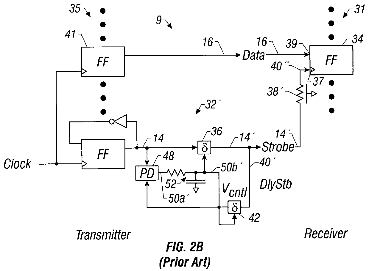
Referring to the drawings, and specifically to FIG. 3, in accordance with an embodiment of the invention, a portion 51 of a DLL 32", which is a modification of the DLL 32 in FIG. 2a (or DLL 32'...


PUM


Abstract

Circuitry added to chips that use source synchronous techniques reduces difficulties associated with testing the chips. The circuitry increases the ability to use source synchronous techniques for data transmission. The circuitry is implemented in a delayed-lock loop (DLL) in either a transmitter (driver) or a receiver. The DLL measures the phase difference between a strobe signal and a delayed strobe signal. The DLL can be externally controlled by a source selectable input which allows the delay of the delayed strobe signal to be varied to test Tsetup and Thold in the receiver without varying the timings of the strobe signal and the data signals supplied to the chips. A timing measurement circuit having the strobe signal, the delayed strobe signal, and reference signals as inputs may be used to calibrate the phase difference between the strobe signal and delayed strobe signal.

Description

1. Field of the InventionThe invention is related to source synchronous techniques, and in particular to the addition of delay circuitry to a chip that uses source synchronous techniques to improve testability of the chip.2. Description of the Related ArtStrobe signals are clock signals that are transmitted with data signals, either simultaneously or after a predetermined delay. The strobe signal is used to time-synchronize data appearing as input signals at a receiver from a driver (transmitter). The use of the strobe signal to indicate when data should be sampled avoids using a clock which is sent to both driver and receiver. If this latter technique is used, then the skew between the two versions of the clock (transmitter and receiver) must be added to the time that each bit is driven from the driver, slowing it down. Sending the clock along with the data eliminates this skew by using the transmitter's clock both to send the data and to send the strobe. Data transfers are referre...

Claims


Application Information

Patent Timeline
Patent Type & Authority Patents(United States)
IPC IPC(8): G01R31/30G01R31/28H03L7/081H03L7/08H03K5/26H03K5/22
CPCG01R31/3016H03K5/26H03L7/0812
Inventor TAYLOR, GREGORY F.
Owner INTEL CORP
Why Eureka
Try Eureka