Digital delay locked loop

a technology of delay loop and lock loop, applied in the direction of pulse automatic control, static storage, instruments, etc., can solve the problems of delay line to increase delay once, increase delay, and then be required

Inactive Publication Date: 2000-07-11
CONVERSANT INTPROP MANAGEMENT INC
View PDF7 Cites 168 Cited by
  • Summary
  • Abstract
  • Description
  • Claims
  • Application Information

AI Technical Summary

Problems solved by technology

The problem translates into a synchronization task between the internal clock, which controls the output path, and the correct edge of the external clock.
In both cases 1 and 3, delay elements are therefore added to the delay line, causing an increase in the delay.
An increase in delay will then be required and the phase detector will cause the delay line to increase delay once again.
As described earlier, once the internal clock is within the time window, the system decreases the delay slightly until the internal clock falls just outside the time window, which in turn will cause the system to once again increase delay.
The repetitive shifting causes internal clock jitter of one delay step while trying to maintain the lock.
However, with smaller element delays more elements are required in the delay line to cover the same minimum-to-maximum delay range.
Furthermore, the small phase detection window characteristic of the phase detector, can cause a loss of lock condition if the system clock itself has jitter which will cause the phase detection window to move away from the lock.
For example, if the internal clock edge falls within the phase detection window and the system clock experienced jitter, the system will bump the internal clock out of the phase detection window and send it searching for a new lock position by starting to increase delay.
The above prior art circuit thus has deficiencies caused by conflicting requirements.
While it has been found to be reliable at start-up of operation, it can easily lose lock when the system clock has jitter, in the manner described above.

Method used


Image

  • Digital delay locked loop
  • Digital delay locked loop
  • Digital delay locked loop

Examples


Embodiment Construction

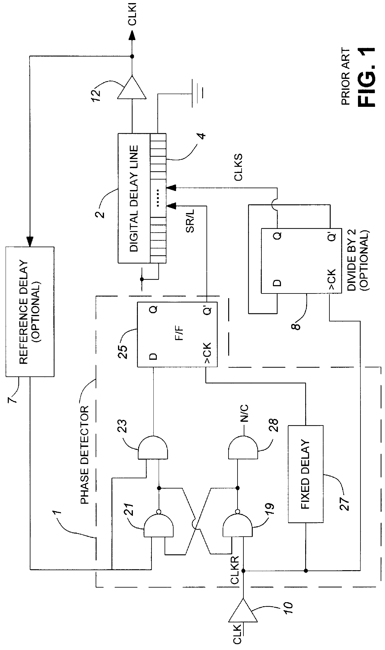
FIG. 3 illustrates the main blocks used to form an embodiment of the present invention. An external main or system clock CLK is applied to a semiconductor device, passing through an input buffer 11 to become reference clock CLKR. Reference clock CLKR is fed from the output of the buffer to a phase detector 25. The outputs of the phase detector are coupled to control circuitry 31 via a clock jitter filter 29 (optional), as well as to other control circuitry 31A controlling a region entry detector 33. The region entry detector 33 inputs into control circuitry 31B to control both an initial phase match detector 39 as well as the shift left / right commands SHL, SHR. The digital delay line 13 receives the shift commands and produces the delayed clock signal CLKD, which in turn is buffered by a high fan-out clock driver 15 to a main internal input / output clock trunk line CLK.sub.-- IO. The signal on the CLK.sub.--IO line is fed back through a reference delay circuit (DLL.sub.-- REF) 17, to...


PUM


Abstract

An improved edge-triggered fully digital delay locked loop (DLL), which maintains reliable synchronization from startup and in spite of system clock jitter is described. An internal clock signal is synchronized with a reference clock signal by propagating the reference clock signal through a variable digital delay path. A wide phase detection region surrounds a selected rising edge of the internal clock signal. The DLL loop is open as long as the internal clock signal and a target edge of the reference clock signal are not simultaneously within the phase detection region. To achieve a DLL locked condition, the variable delay is increased from a minimum setting until the edge of the phase detection region is shifted in time just past the target edge of the reference clock. Once the DLL loop has been closed, a clock jitter filter is enabled to reject reference clock jitter effects on the DLL locked condition. A digital phase detector controls the delay line propagation delay to establish synchronization between the internal clock and the reference clock. Unused delay elements within the variable delay path are deactivated to save power.

Description

This invention relates to digital delay locked loops for use in high frequency clock synchronization applications.BACKGROUND TO THE INVENTIONIn synchronous dynamic random access memory (SDRAM) applications, as frequencies approach 200 MHz, the inherent analog delay between an external, system or reference clock and the time output data is valid, is becoming a crucial constraint. Such a delay of e.g. 4-10 ns is large enough to make a following clock cycle overlap the data, i.e. the delay becomes large enough for data not to be ready at the output during one cycle, and it essentially becomes "off-sync". This inherent internal delay must therefore be accelerated according to the necessary frequency but in a controlled fashion. The problem translates into a synchronization task between the internal clock, which controls the output path, and the correct edge of the external clock.Analog delay locked loops have been employed in the past to perform the synchronization, which are comprised ...

Claims


Application Information

Patent Timeline
Patent Type & Authority Patents(United States)
IPC IPC(8): G11C7/00G11C7/22H03L7/081H03L7/08H03L7/089
CPCG11C7/22H03L7/0814H03L7/089H03L7/0816
Inventor MILLAR, BRUCE
Owner CONVERSANT INTPROP MANAGEMENT INC
Why Eureka
Try Eureka