Forward body biased field effect transistor providing decoupling capacitance

a field effect transistor and forward body technology, applied in pulse generators, instruments, pulse techniques, etc., can solve the problems of mosfets posing a major barrier to achieving performance and power goals, affecting the development cost of future process technologies, and affecting the performance and power of mosfets

Inactive Publication Date: 2000-08-08
INTEL CORP
View PDF22 Cites 75 Cited by
  • Summary
  • Abstract
  • Description
  • Claims
  • Application Information

AI Technical Summary

Problems solved by technology

As the minimum feature size scales below, for example, 0.18 micrometers, the available design space for construction of a MOSFET which provides sufficient drive current at low supply voltages while maintaining adequate SCE, DIBL, and PT immunity becomes severely restricted.
These design challenges for ultra-small bulk MOSFETs can pose a major barrier to achieving the performance and power goals in future generations of microprocessor, communication, and memory chips.
In addition, these design difficulties can cause the development cost of future process technologies to escalate by large amounts.

Method used


Image

  • Forward body biased field effect transistor providing decoupling capacitance
  • Forward body biased field effect transistor providing decoupling capacitance
  • Forward body biased field effect transistor providing decoupling capacitance

Examples


Embodiment Construction

. Voltage Source Examples

D. Multiple Vt Circuits

E. Multiple Wells

F. Forward Body Bias from the Supply and Ground Voltage Nodes

G. Soft Error Rate

H. Other Advantages of Forward Body Bias

I. Process of Manufacturing and Structure of Some Preferred Transistors

J. Additional Information

Reference in the specification to "one embodiment" or "an embodiment" means that a particular feature, structure, or characteristic described in connection with the embodiment is included in at least one embodiment of the invention. The appearances of the phrase "in one embodiment" or "an embodiment" in different places in the specification are not necessarily all referring to the same embodiment.

A. Forward Body Bias

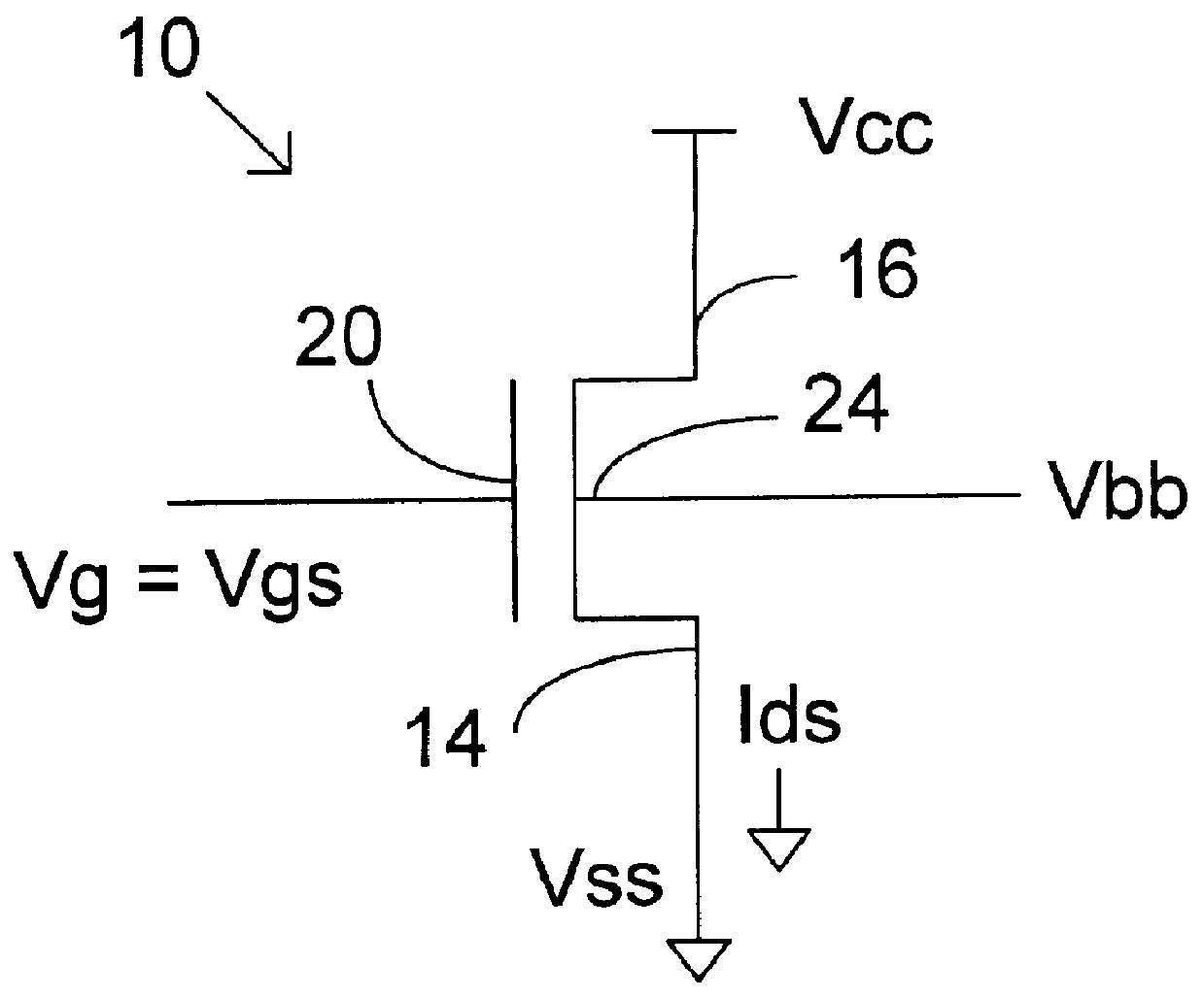
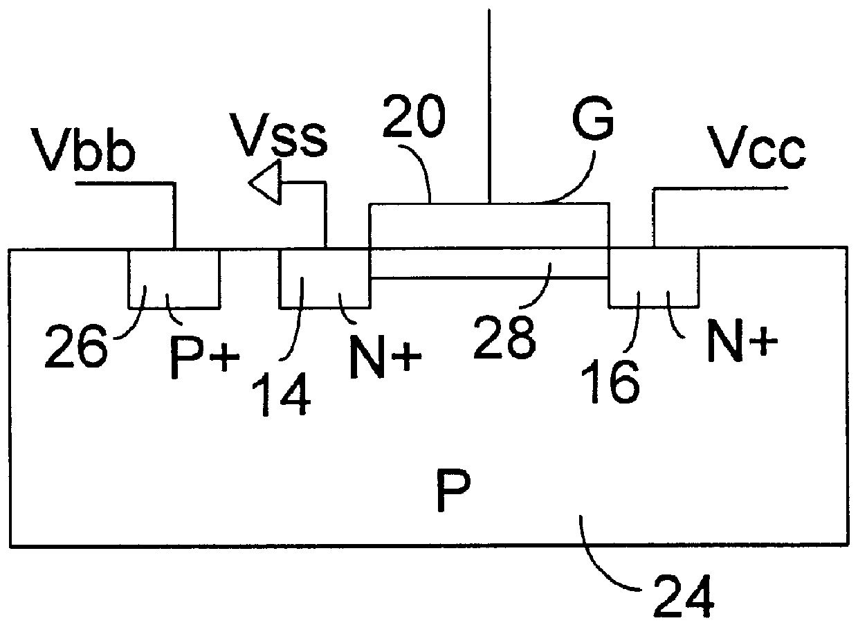
Referring to FIGS. 1 and 2, a MOSFET transistor 10 includes a source 14 at a reference voltage Vss (which may be earth ground), a drain 16 receiving a source voltage Vcc (often called VDD), and a gate 20 receiving a gate voltage Vg. (In practice, there may be resistors, transistors, or other elem...


PUM


Abstract

In one embodiment of the invention, a semiconductor circuit includes a first group of field effect transistors that are forward body biased and have threshold voltages and a second group of field effect transistors that are not forward body biased and have threshold voltages that are higher than the threshold voltages of the first group of field transistors. In another embodiment of the invention, a semiconductor circuit includes first and second groups of field effect transistors. The circuit includes voltage source circuitry to provide voltage signals to bodies of the first group of field effect transistors to forward body bias the transistors of the first group. When the voltage signals are applied, the transistors of the first group have lower threshold voltages than do the transistors of the second group, except that there may be unintentional variations in threshold voltages due to parameter variations. Other aspects of the invention include forward biased decoupling transistors and a method of testing for leakage.

Description

1. Technical Field of the InventionThe present invention relates to semiconductor circuits and, more particularly, to semiconductor circuits in which the bodies of at least some transistors are forward-biased.2. Description of Prior ArtIn conventional static, dynamic, and differential complementary metal oxide semiconductor (CMOS) logic and memory circuits, an n-Channel metal oxide semiconductor field effect transistor (MOSFET) (nMOS transistor) or a p-Channel MOSFET (pMOS transistor) is used with its body terminal connected to the ground or supply voltage node, respectively. Other circuit schemes have been proposed where a reverse bias is applied statically or dynamically to the body node of a MOSFET to reduce subthreshold leakage current when the MOSFET is not switching. In these schemes, the body of the pMOS transistor is connected to a voltage source larger (more positive) than the supply voltage, and the body of the nMOS transistor is connected to a voltage source smaller (more...

Claims


Application Information

Patent Timeline
Patent Type & Authority Patents(United States)
IPC IPC(8): H01L29/02H01L29/10H01L27/085H01L27/092H03K19/0948H03L7/081H03L7/099
CPCH01L27/0928H01L29/1087H03K19/0948H03L7/0812H03L7/0995H01L21/823807H01L21/823892H01L27/092
Inventor DE, VIVEK K.KESHAVARZI, ALINARENDRA, SIVA G.BORKAR, SHEKHAR Y.
Owner INTEL CORP
Why Eureka
Try Eureka