Layout design method and system for an improved place and route

a layout design and integrated circuit technology, applied in computer aided design, program control, instruments, etc., can solve the problems of inability to estimate, rate cannot be used as information to optimize at the stage of automatic placement or automatic routing, and is unsuitable for information to optimize each n

Inactive Publication Date: 2000-08-29
KK TOSHIBA
View PDF19 Cites 61 Cited by
  • Summary
  • Abstract
  • Description
  • Claims
  • Application Information

AI Technical Summary

Problems solved by technology

In this manner, in the design of the semiconductor integrated circuit in the prior art, there has been a problem such that, since the layout design and the logic design must be carried out once again according to the verification result, a design term has been extended.
However, the method in which the capacitances between adjacent wirings are considered at the stage before the cell placement have large estimation error and therefore is unsuitable for information to optimize each net.
On the other hand, by the method in which the adjacent rate and the intersecting rate are estimated after the detailed routing, such rates cannot be used as information

Method used


Image

  • Layout design method and system for an improved place and route
  • Layout design method and system for an improved place and route
  • Layout design method and system for an improved place and route

Examples


embodiment 1

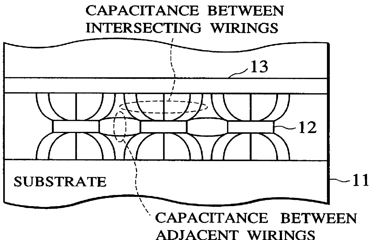
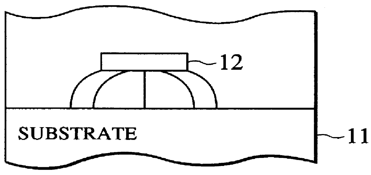
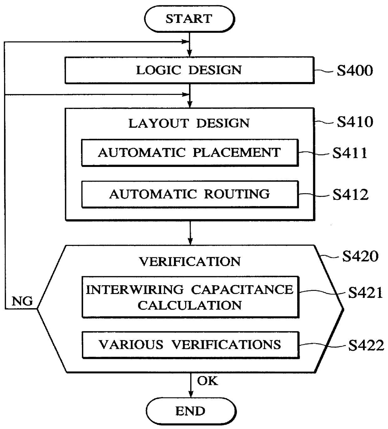
FIG. 5 is a flowchart showing the process carried out by a means 202 for calculating capacitances between adjacent wirings of the present invention. First, a routing congestion is calculated (step S110). Here a semiconductor chip whose layout placement has been finished is segmented into previously given m.times.n regions (m, n are arbitrary integers) and the routing congestion for each side of the region is calculated in respective regions. As the first method of calculating the routing congestion, the technology concerning the method which is able to estimate the routing congestion without the global routing has been disclosed (Patent Application Publication (KOKAI) Hei 8-247399, Applicant: Toshiba Corporation). In this method, rectangles are set on all nets and then the routing congestion can be estimated by the stochastic approach. According to this method, the routing congestion can be estimated with good accuracy and at high speed without actual wirings. As the second method, ...

embodiment 2

Next, a second embodiment of the present invention will be explained hereinbelow. FIG. 8 shows the expected value .alpha.' of the adjacent wiring length three-dimensionally, wherein an ordinate denotes the adjacent distance d and an abscissa denotes the routing congestion. As shown in FIG. 8, the expected value of the adjacent wiring length with respect to the routing congestion grows smaller as the adjacent wire spacing d becomes wider. In other words, the expected value of the adjacent wiring length with respect to the routing congestion is varied according to the adjacent wire spacing d. Therefore, it is to be noted that, if the adjacent wire spacing d is included as the variable, the capacitances between adjacent wirings can be calculated with better precision.

In the present embodiment, in the process in step S132 in FIG. 5, the expected value of the adjacent wiring length is calculated and, for the objective wiring, the expected value .alpha.' of the adjacent wiring length per ...

embodiment 3

Next, a third embodiment of the present invention will be explained hereinbelow. In this embodiment, the capacitance between intersecting wirings will be calculated. More particularly, the intersecting number is calculated. For this, the intersecting rate of respective wiring layers is calculated based on the routing congestion according to the above function f. In turn, a sum of capacitances between intersecting wirings for respective wiring layers is assumed as the capacitance between intersecting wirings with respect to the wiring. FIG. 9 is a flowchart showing the process carried out by the means 202 for calculating capacitances between intersecting wirings according to the present embodiment. At first, the routing congestion is calculated (step S210). Then, the schematic wiring routes are predicted for respective nets (step S220). Because these processes may be conducted as the same processes as those in the first embodiment, their explanation will be omitted.

Then, the intersec...


PUM


Abstract

A layout design method and system for a semiconductor integrated circuit improves circuit performances related to operated frequency and power consumption by improved placement and routing. The method features an intersecting wiring predicting step that predicts the number of the intersecting wirings based on predicted wiring routes and an intersecting wiring capacitance calculating step that calculates the capacitances between the intersecting wirings.

Description

1. Field of the InventionThe present invention relates to a semiconductor integrated circuit design system, a semiconductor integrated circuit design method, a computer-readable recording medium for recording a semiconductor integrated circuit design program, and a method of manufacturing the semiconductor integrated circuit and, more particularly, a technology for carrying out a semiconductor integrated circuit design effectively by estimating interwiring capacitances with good precision prior to routing process.2. Description of the Related ArtIn the semiconductor integrated circuit in the deep submicron generation, it would be anticipated that capacitances between adjacent wirings and capacitances between intersecting wirings are increased. FIGS. 1A and 1B are views illustrating the capacitances between adjacent wirings and the capacitances between intersecting wirings. FIG. 1A shows a sectional model illustrative of a simple parallel plates in an ordinary semiconductor integrate...

Claims


Application Information

Patent Timeline
IPC IPC(8): G06F17/50H01L21/82
CPCG06F17/5072G06F30/392
Inventor MINAMI, FUMIHIROMUROFUSHI, MASAKO
Owner KK TOSHIBA
Why Eureka
Try Eureka