

High frequency amplifier circuit
a high-frequency amplifier and circuit technology, applied in the direction of automatic tone/bandwidth control, amplifier modification to reduce non-linear distortion, gain control, etc., can solve the problems of distortion for generated, difficult to optimize simultaneously, and difficult to compensate for
- Summary
- Abstract
- Description
- Claims
- Application Information
AI Technical Summary
Problems solved by technology
Method used
Image

Examples
first embodiment
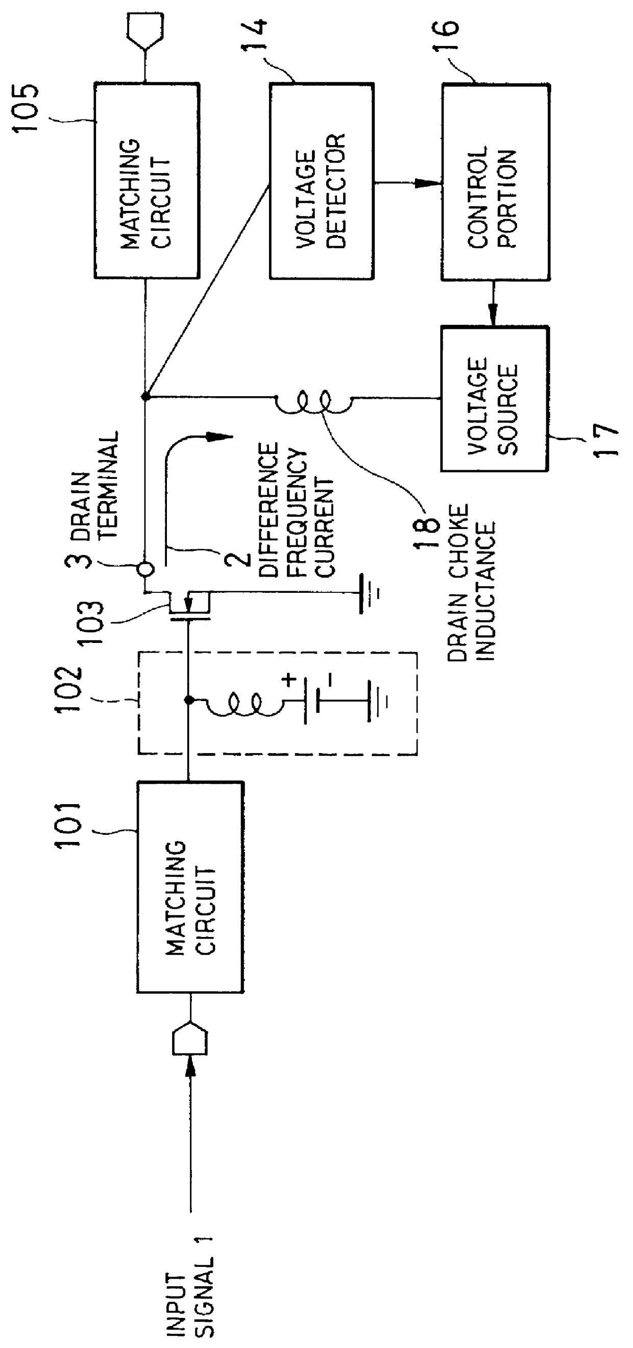
FIG. 1 is a block diagram showing a construction of a high frequency amplifier circuit according to the present invention, which constitutes the best mode of the present invention.
A high frequency amplifier circuit includes an input matching circuit 101, a gate bias circuit 102, a high frequency amplifying MOSFET 103, a drain choke inductance 18, a voltage source 17 supplying a drain power source of the MOSFET 103, a voltage detector 14 detecting a voltage at a drain, a control portion 16 controlling a voltage of the voltage source 17 depending upon a voltage detected by the voltage detector 14.
The drain choke inductance 18 is a sufficiently high inductance with respect to a signal which is amplified (a signal corresponding to an input signal spectrum 4, see FIG. 20). The inductance represents low impedance with respect to a signal having a frequency lower than a signal to be amplified as a difference frequency (a signal corresponding to a difference frequency spectrum 6, see FIG. 2...
second embodiment
the high frequency amplifier circuit comprises the input matching circuit 101, the gate bias circuit 102, the high frequency amplifying MOSFET 103, the drain choke inductance 18, a current detector 21 for detecting a drain current, the voltage source 17 for supplying a power source to the drain of the MOSFET 103, a control portion controlling the voltage of the voltage source 17 depending upon a current detected by the current detector 21, and the output matching circuit 105.
Next, operation will be discussed.
A current flowing through the drain power source supply circuit is detected by the current detector 21. The detected data is input to the control portion 22. The control portion 22 predicts a difference frequency voltage component of the input signal 1 generated at the drain terminal 3 from the current flowing through the drain power supply circuit.
A method for predicting the difference frequency voltage component from the current input to the current detector 21 is similar to t...
sixth embodiment
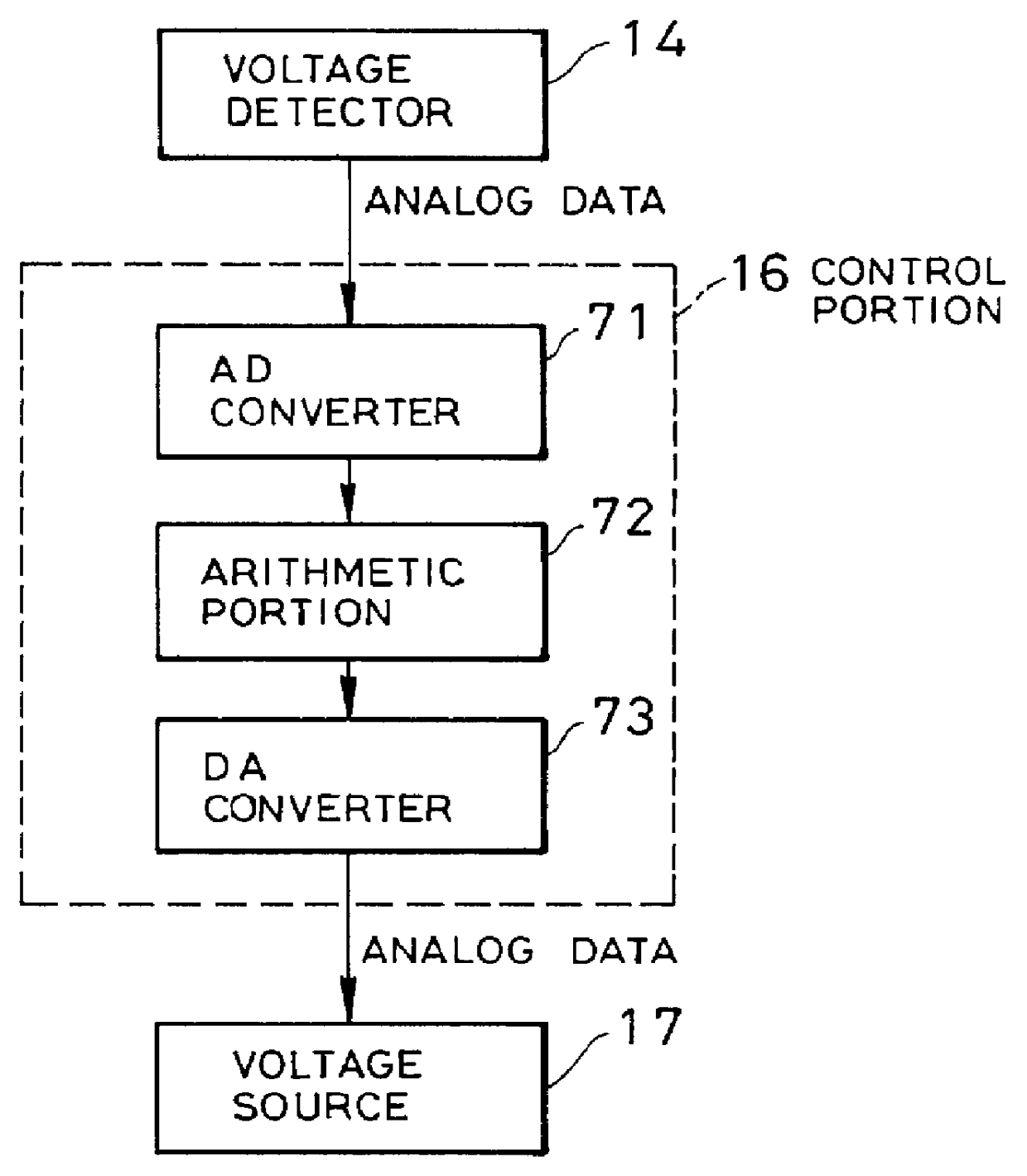
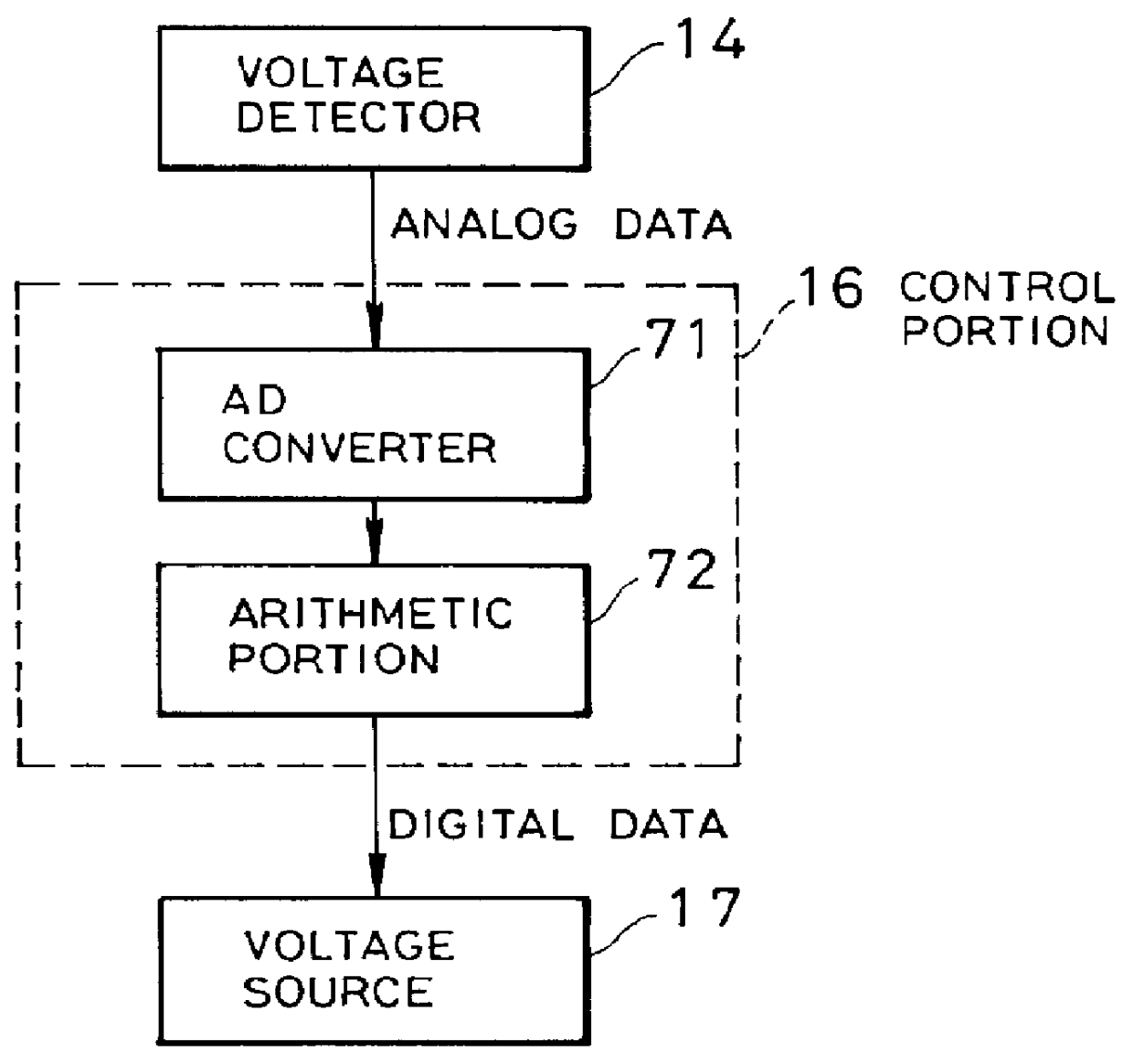
Next, embodiments of the control portion 22 will be discussed. FIGS. 6 to 8 are block diagrams showing a construction of the fourth to sixth embodiment of the control portion. It should be noted that, for convenience, the current detector 21 and the voltage source 17 are illustrated in FIGS. 6 to 8.
At first, the fourth embodiment of the control portion will be discussed with reference to FIG. 6. The control portion 22 comprises an AD converter 81 digital converting the analog signal, an arithmetic portion 82 performing arithmetic operation for the data output from the AD converter 81 and a DA converter 83 converting the result of arithmetic operation in the arithmetic portion 82 into an analog data.
Next, operation will be discussed. An analog data of the instantaneous value of the current output from the current detector 21 is converted into the digital data by the AD converter 81. Then, the control signal is determined in the arithmetic portion 82. After determination, the control ...
PUM
 Abstract
Description
Claims
Application Information