Multipurpose cap layer dielectric
- Summary
- Abstract
- Description
- Claims
- Application Information
AI Technical Summary
Benefits of technology
Problems solved by technology
Method used
Image
Examples
Embodiment Construction
The process steps and structures described below do not form a complete process flow for manufacturing integrated circuits. The present invention can be practiced in conjunction with integrated circuit fabrication techniques currently used in the art, and only so much of the commonly practiced process steps are included as are necessary for an understanding of the present invention. The figures representing cross-sections of portions of an integrated circuit device during fabrication are not drawn to scale, but instead are drawn so as to illustrate the important features of the present invention.
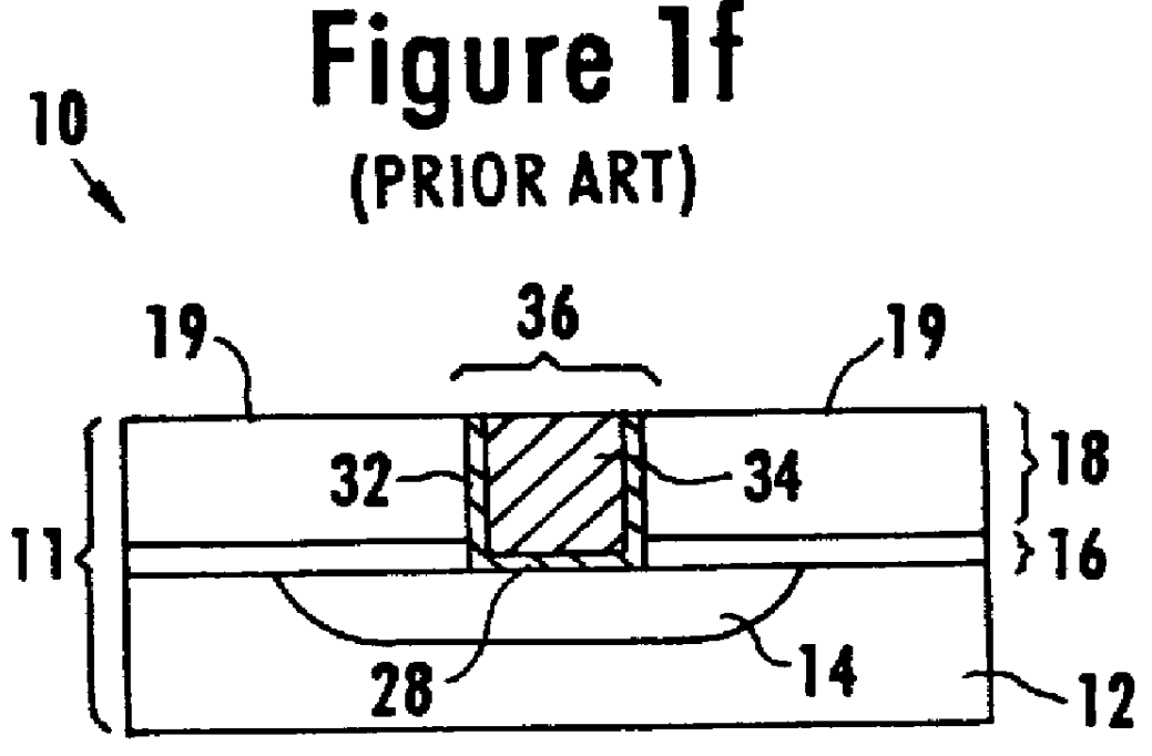
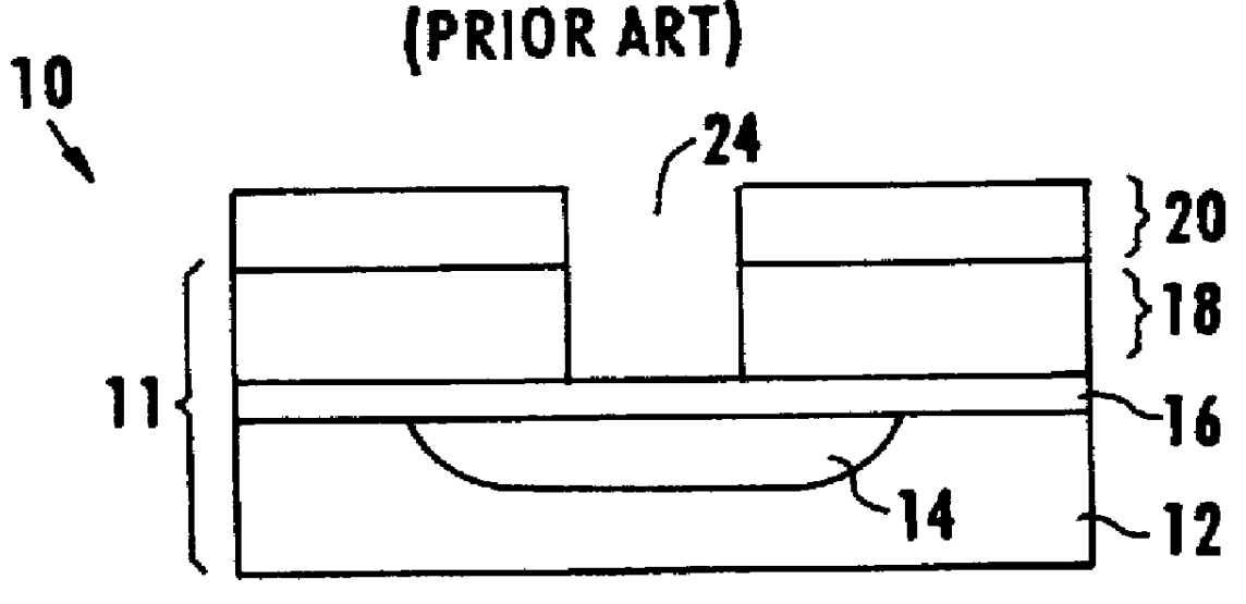
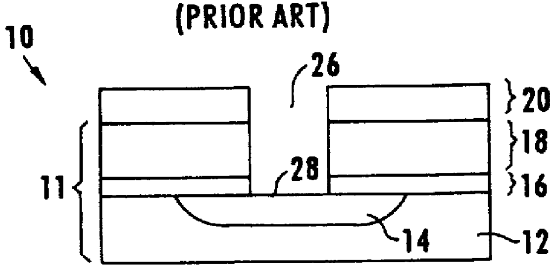
With this in mind, the limitations of the prior art methods and arrangements will first be described as depicted in FIGS. 1a through 1g. FIG. 1a depicts a cross-section of a portion 10 of a typical semiconductor wafer that has been prepared for a conventional local interconnect formation process. Portion 10 includes a wafer stack 11 having a substrate 12, a stop layer 16 and a dielectric lay...
PUM
 Abstract
Description
Claims
Application Information
 - R&D Engineer
- R&D Manager
- IP Professional
- Industry Leading Data Capabilities
- Powerful AI technology
- Patent DNA Extraction
Browse by: Latest US Patents, China's latest patents, Technical Efficacy Thesaurus, Application Domain, Technology Topic, Popular Technical Reports.
© 2024 PatSnap. All rights reserved.Legal|Privacy policy|Modern Slavery Act Transparency Statement|Sitemap|About US| Contact US: help@patsnap.com


