Electro-optical device and method of fabricating same

a technology of optical devices and liquid crystals, applied in the direction of optics, semiconductor devices, instruments, etc., can solve the problems of deteriorating the displayed image, low aperture ratio, and affecting the contrast of the displayed imag

Inactive Publication Date: 2000-09-12
SEMICON ENERGY LAB CO LTD
View PDF4 Cites 151 Cited by
  • Summary
  • Abstract
  • Description
  • Claims
  • Application Information

AI Technical Summary

Problems solved by technology

This varies the electrooptical characteristics of the liquid crystal material, thus impairing the contrast of the displayed image.
That is, the conventional structure has the disadvantage that the aperture ratio is low.
When a voltage is applied, the edges

Method used


Image

  • Electro-optical device and method of fabricating same
  • Electro-optical device and method of fabricating same
  • Electro-optical device and method of fabricating same

Examples


embodiment 2

The present embodiment differs from the configuration shown in FIG. 2 in that a black matrix is formed only above the TFTS. The greatest feature of the present embodiment is that the black matrix is replaced by gate lines and data lines.

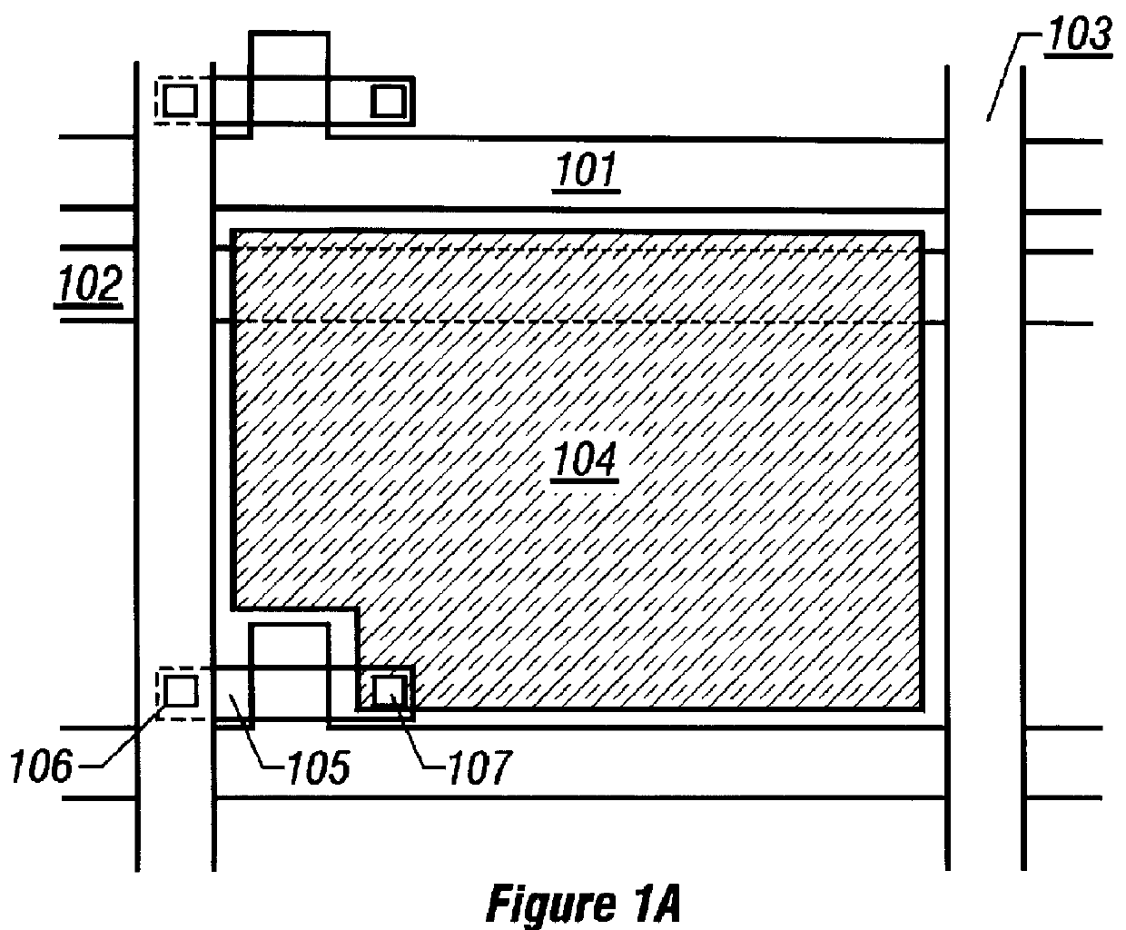
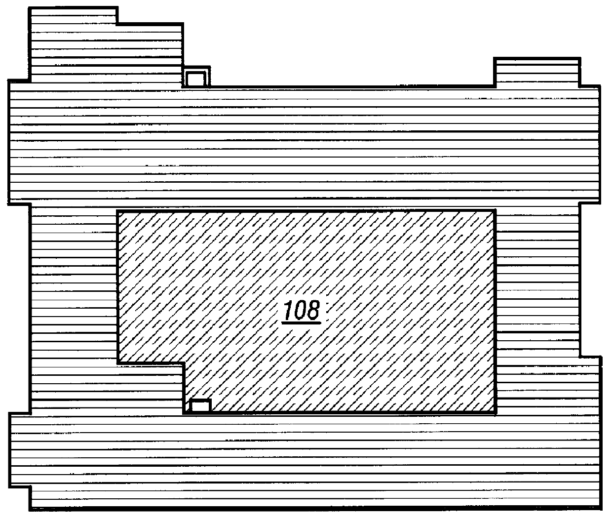
In the configuration shown in FIG. 5, there are shown gate lines 501, data lines 502, a semiconductor layer 503 forming the active layer of TFTs, the black matrix 504, pixel electrodes 505, and contacts 506 between the semiconductor layer 503 and the pixel electrodes 505.

It is to be noted that in the present embodiment, the edges of the pixel electrodes 505 overlap the gate lines 501 and the data lines 502. In this case, parasitic capacitances which would normally be created between the gate lines 501 and the pixel electrodes 505 and between the data lines 502 and the pixel electrodes 505 present problems.

In the present embodiment, the second interlayer dielectric film 315 acting as the dielectric layer of each parasitic capacitor is made from a mate...

embodiment 3

In the present embodiment, the LPD (liquid phase deposition) used in fabricating the second or third interlayer dielectric film in Embodiment 1 is described. The LPD is a means for obtaining a desired film by dissolving an organic resinous material or inorganic material in a solvent, applying the resulting solution to a substrate to be processed, and baking the applied solution. The process sequence for fabricating the pixel TFTs and driver TFTs has been already described in Embodiment 1 and so will not be described now.

The manner in which a film is formed by LPD is described below briefly. In the description provided below, the film is made of silicon oxide-based material (SiO.sub.x) that is an inorganic material. Another example of the inorganic material of the film is SiOF having a relative dielectric constant of 3.2-3.3. A transparent polyimide having a relative dielectric constant of 2.8-3.4 can be used as an organic resinous material.

First, an H.sub.2 SiF.sub.6 solution is pre...

embodiment 4

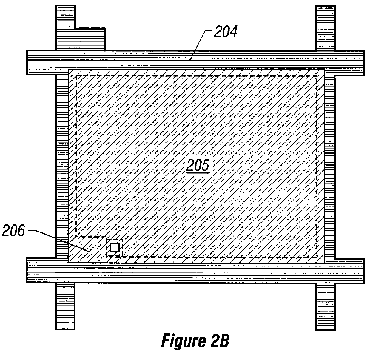
In the present embodiment, a second retaining capacitance is used in addition to the retaining capacitance (referred to herein as the first retaining capacitance) according to the present invention. This second retaining capacitance has been invented, based on our research.

This second retaining capacitance is formed by gate lines and pixel electrodes via a first interlayer dielectric film. This will be described in detail by referring to FIG. 6.

FIG. 6 is a top view of pixel regions where the first retaining capacitance (region surrounded by broken line 601) according to the invention and the aforementioned second retaining capacitance (region surrounded by broken line 602) according to the invention are used in conjunction (in combination).

Shown in this figure are gate lines 603, data lines 604, and a semiconductor layer 605 forming the active layer of TFTS.

The fabrication sequence for the first retaining capacitance 601 has been already described in Embodiment 1. A process sequence...


PUM


Abstract

An active matrix liquid crystal display having a high aperture ratio is provided. Retaining capacitors are created between a black matrix and pixel electrodes via a dielectric layer made from an organic resinous material or inorganic material. Those regions of the black matrix which cover TFTs are fully utilized. Therefore, wider area can be used to display an image than heretofore. In the present invention, the difference in relative dielectric constant between different dielectric layers is employed. Therefore, retaining capacitors can be created without the need to take account of parasitic capacitance.

Description

1. Field of the InventionThe present invention relates to a liquid crystal display construction including semiconductor devices which are made of a crystalline silicon film and act as control devices and, more particularly, to the construction of pixel regions of an active matrix liquid crystal display.2. Description of the Related ArtIn recent years, techniques for fabricating thin-film transistors (TFTS) on cheap glass substrates have evolved rapidly because there is an increasing demand for active matrix liquid crystal displays.In an active matrix liquid crystal display, millions of pixels are arranged in rows and columns. At least one TFT is disposed at each of these pixels. Electric charge going into and out of each pixel electrode is controlled by the switching function of the TFT.A liquid crystal material is sandwiched between each pixel electrode and a counter electrode to form one kind of capacitor. Accordingly, the electrooptical characteristics of the liquid crystal mater...

Claims


Application Information

Patent Timeline
IPC IPC(8): G02F1/13G02F1/1362H01L21/02H01L21/70H01L29/66H01L21/336H01L21/84H01L27/12H01L29/786H01L21/77
CPCG02F1/136209G02F1/136213H01L29/66757H01L29/78621H01L27/1255G02F1/1343G02F1/136
Inventor YAMAZAKI, SHUNPEIKOYAMA, JUNYAMAGUCHI, NAOAKIAWANE, KATUNOBUFUNADA, FUNIAKIYAMAMOTO, YOSHITAKA
Owner SEMICON ENERGY LAB CO LTD
Why Eureka
Try Eureka