

Organic electroluminescence device
a technology of electroluminescence and organic material, which is applied in the direction of luminescnet screens, discharge tubes, natural mineral layered products, etc., can solve the problems of deterioration of color purity, failure to disclose the possibility of improving the color purity of the device, and reducing efficiency
- Summary
- Abstract
- Description
- Claims
- Application Information
AI Technical Summary
Problems solved by technology
Method used
Image

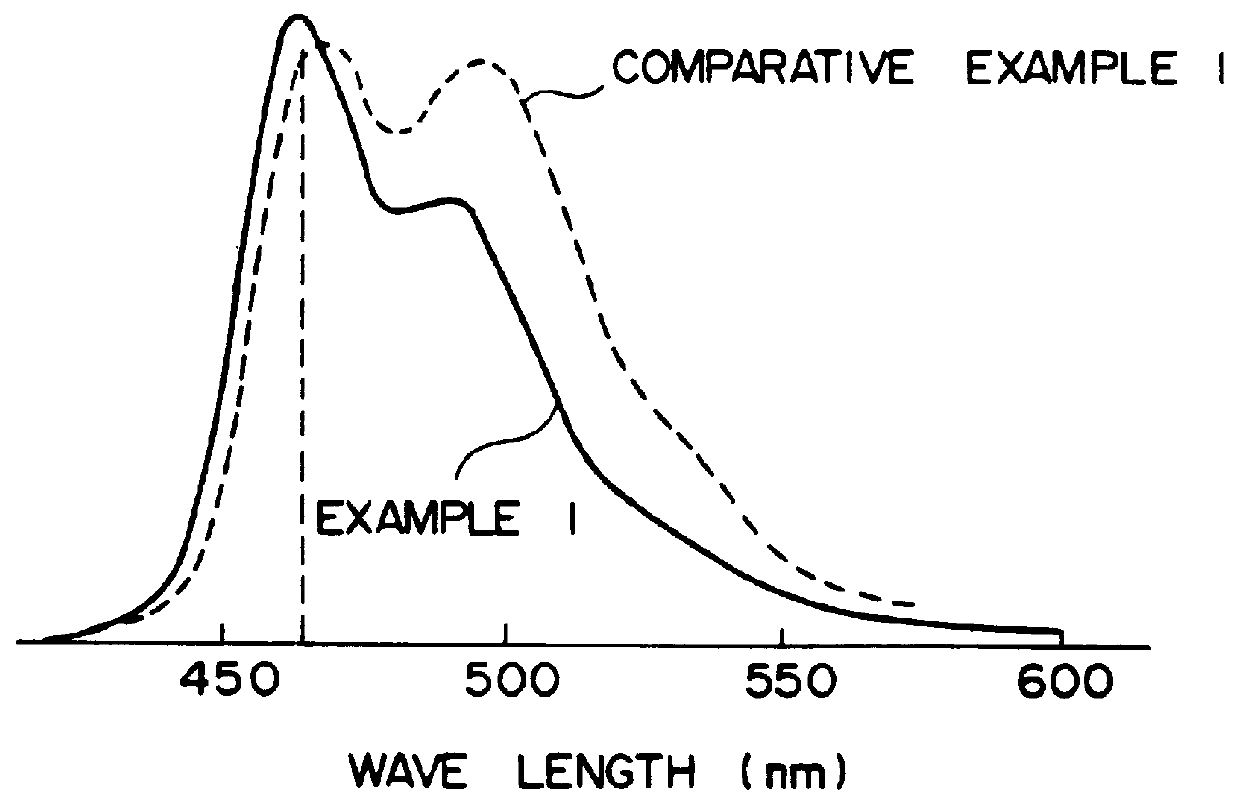
Examples
examples 4 to 6
(1) Preparation of a Device
EL devices having the thickness shown in Table 5 were prepared by the same method as that used in Example 1, except the following points: in Example 4, an ITO having a high refractive index of 1.92 was used in place of the ITO used in Example 1; in Example 5, a TiO.sub.2 layer having a refractive index of 2.4 used as the underlayer of a high refractivity was formed to the thickness of 48 nm between the substrate and the ITO layer by the vacuum vapor deposition; and in Example 6, a MgF.sub.2 layer having a refractive index of 1.38 used as the underlayer of a low refractivity was formed to the thickness of 80 nm between the substrate and the ITO layer by the vacuum vapor deposition.
The thickness of the layers are shown in Table 5, and .lambda. and m are shown in Table 6.
TABLE 3
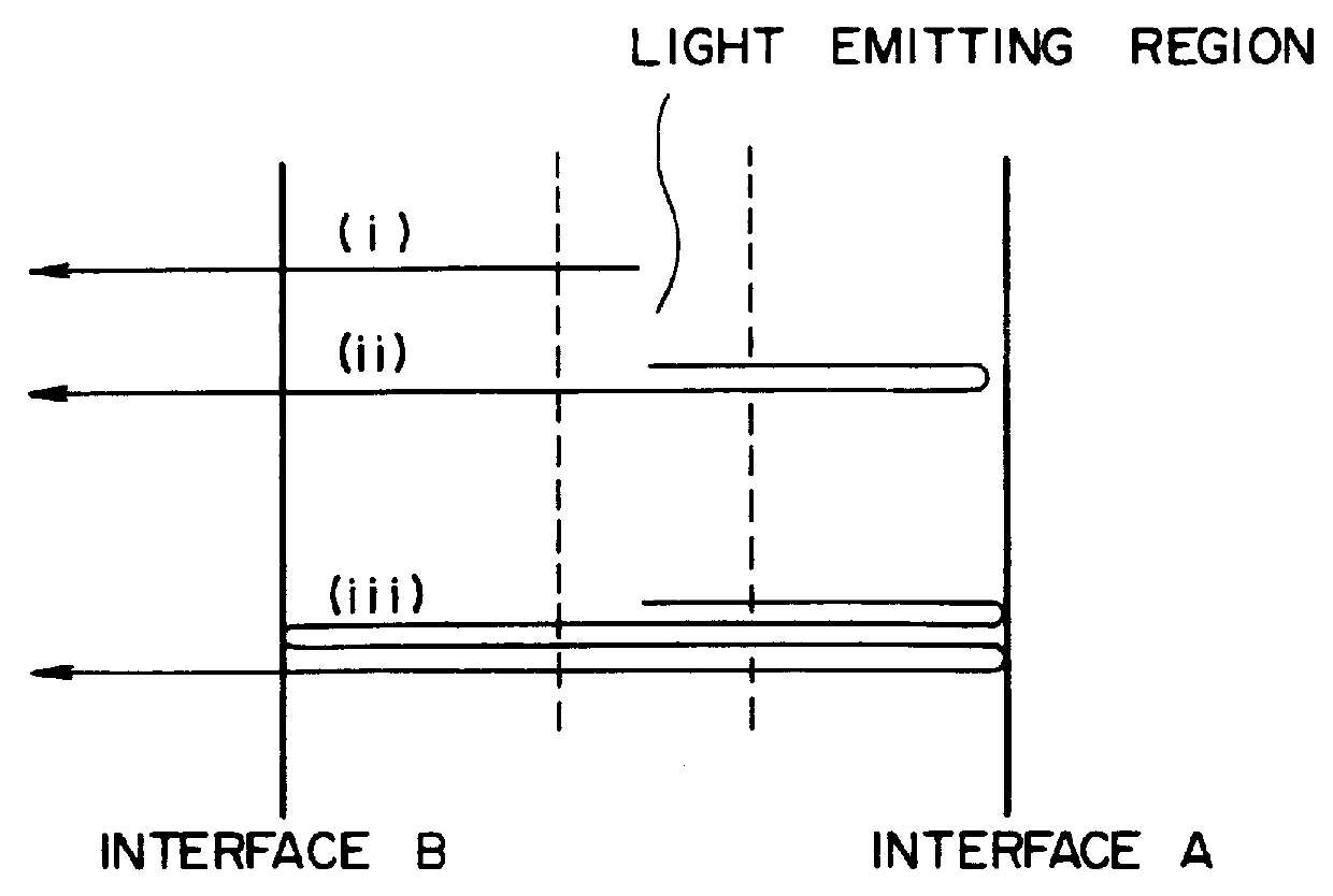
In Example 5, the reflection took place at the interface of the underlayer of a high refractivity and the transparent electrode, and the optical thickness is [(nd).sub.1 +(nd).sub.3 ]....
PUM
| Property | Measurement | Unit |
|---|---|---|
| Nanoscale particle size | aaaaa | aaaaa |
| Nanoscale particle size | aaaaa | aaaaa |
| Nanoscale particle size | aaaaa | aaaaa |
Abstract
Description
Claims
Application Information